
 | ||
Graphene (/ˈɡræf.iːn/) is an allotrope of carbon in the form of a two-dimensional, atomic-scale, hexagonal lattice in which one atom forms each vertex. It is the basic structural element of other allotropes, including graphite, charcoal, carbon nanotubes and fullerenes. It can be considered as an indefinitely large aromatic molecule, the ultimate case of the family of flat polycyclic aromatic hydrocarbons.
Contents
- Definition
- History
- Properties
- Structure
- Chemical
- Electronic
- Electronic spectrum
- Single atom wave propagation
- Electron transport
- Dirac fluid
- Anomalous quantum Hall effect
- Strong magnetic fields
- Casimir effect
- Van der Waals force
- Massive electrons
- Optical
- Saturable absorption
- Nonlinear Kerr effect
- Excitonic
- Stability
- Thermal conductivity
- Melting point
- Mechanical
- Fracture toughness
- Spin transport
- Magnetic
- Biological
- Substrate
- Monolayer sheets
- Bilayer
- Superlattices
- Nanoribbons
- Quantum dots
- Oxide
- Chemical modification
- Ligandcomplex
- Fiber
- 3D
- Gyroid
- Molded
- Aerogel
- Pillared
- Reinforced
- Nanocoil
- Production
- Exfoliation
- Sonication
- Molten salts
- Electrochemical synthesis
- Hydrothermal self assembly
- Epitaxy
- Metal substrates
- Sodium ethoxide pyrolysis
- Roll to roll
- Cold wall
- Nanotube slicing
- Carbon dioxide reduction
- Spin coating
- Supersonic spray
- Laser
- Microwave assisted oxidation
- Ion implantation
- Heated vegetable oil
- Analogs
- Applications
- Health risks
- References
Graphene has many unusual properties. It is about 200 times stronger than the strongest steel. It efficiently conducts heat and electricity and is nearly transparent. Graphene shows a large and nonlinear diamagnetism, greater than graphite and can be levitated by neodymium magnets.
Scientists have theorized about graphene for years. It has unintentionally been produced in small quantities for centuries, through the use of pencils and other similar graphite applications. It was originally observed in electron microscopes in 1962, but only studied while supported on metal surfaces. The material was later rediscovered, isolated, and characterized in 2004 by Andre Geim and Konstantin Novoselov at the University of Manchester. Research was informed by existing theoretical descriptions of its composition, structure, and properties. This work resulted in the two winning the Nobel Prize in Physics in 2010 "for groundbreaking experiments regarding the two-dimensional material graphene."
The global market for graphene reached $9 million by 2012 with most sales in the semiconductor, electronics, battery energy, and composites industries.
Definition
"Graphene" is a combination of "graphite" and the suffix -ene, named by Hanns-Peter Boehm, who described single-layer carbon foils in 1962.
The term graphene first appeared in 1987 to describe single sheets of graphite as a constituent of graphite intercalation compounds (GICs); conceptually a GIC is a crystalline salt of the intercalant and graphene. The term was also used in early descriptions of carbon nanotubes, as well as for epitaxial graphene and polycyclic aromatic hydrocarbons (PAH). Graphene can be considered an "infinite alternant" (only six-member carbon ring) polycyclic aromatic hydrocarbon.
The IUPAC compendium of technology states: "previously, descriptions such as graphite layers, carbon layers, or carbon sheets have been used for the term graphene... it is incorrect to use for a single layer a term which includes the term graphite, which would imply a three-dimensional structure. The term graphene should be used only when the reactions, structural relations or other properties of individual layers are discussed."
Geim defined "isolated or free-standing graphene" as "graphene is a single atomic plane of graphite, which – and this is essential – is sufficiently isolated from its environment to be considered free-standing." This definition is narrower than the IUPAC definition and refers to cloven, transferred and suspended graphene. Other forms such as graphene grown on various metals, can become free-standing if, for example, suspended or transferred to silicon dioxide (SiO
2) or silicon carbide.
History
In 1859 Benjamin Collins Brodie became aware of the highly lamellar structure of thermally reduced graphite oxide.
The structure of graphite was identified in 1916 by the related method of powder diffraction. It was studied in detail by Kohlschütter and Haenni in 1918, who described the properties of graphite oxide paper. Its structure was determined from single-crystal diffraction in 1924.
The theory of graphene was first explored by Wallace in 1947 as a starting point for understanding the electronic properties of 3D graphite. The emergent massless Dirac equation was first pointed out by Semenoff, DiVincenzo and Mele. Semenoff emphasized the occurrence in a magnetic field of an electronic Landau level precisely at the Dirac point. This level is responsible for the anomalous integer quantum Hall effect.
The earliest TEM images of few-layer graphite were published by Ruess and Vogt in 1948. Later, single graphene layers were observed directly by electron microscopy. Before 2004 intercalated graphite compounds were studied under a transmission electron microscope (TEM). Researchers occasionally observed thin graphitic flakes ("few-layer graphene") and possibly even individual layers. An early, detailed study on few-layer graphite dates to 1962 when Boehm reported producing monolayer flakes of reduced graphene oxide.
Starting in the 1970s single layers of graphite were grown epitaxially on top of other materials. This "epitaxial graphene" consists of a single-atom-thick hexagonal lattice of sp2-bonded carbon atoms, as in free-standing graphene. However, significant charge transfers from the substrate to the epitaxial graphene, and in some cases, the d-orbitals of the substrate atoms hybridize with the π orbitals of graphene, which significantly alters the electronic structure of epitaxial graphene.
Single layers of graphite were observed by TEM within bulk materials, in particular inside soot obtained by chemical exfoliation. Efforts to make thin films of graphite by mechanical exfoliation started in 1990, but nothing thinner than 50 to 100 layers was produced before 2004.
Initial attempts to make atomically thin graphitic films employed exfoliation techniques similar to the drawing method. Multilayer samples down to 10 nm in thickness were obtained. Earlier researchers tried to isolate graphene starting with intercalated compounds, producing very thin graphitic fragments (possibly monolayers). Neither of the earlier observations was sufficient to launch the "graphene gold rush" that awaited macroscopic samples of extracted atomic planes.
One of the first patents pertaining to the production of graphene was filed in October 2002 and granted in 2006. It detailed one of the first large scale graphene production processes. Two years later, in 2004 Geim and Novoselov extracted single-atom-thick crystallites from bulk graphite. They pulled graphene layers from graphite and transferred them onto thin silicon dioxide (SiO
2) on a silicon wafer in a process called either micromechanical cleavage or the Scotch tape technique. The SiO
2 electrically isolated the graphene and weakly interacted with it, providing nearly charge-neutral graphene layers. The silicon beneath the SiO
2 could be used as a "back gate" electrode to vary the charge density in the graphene over a wide range. US patent 6667100, filed in 2002, describes how to process expanded graphite to achieve a graphite thickness of 0.00001" (one hundred-thousandth) of an inch. The key to success was high-throughput visual recognition of graphene on a properly chosen substrate, which provides a small but noticeable optical contrast.
The cleavage technique led directly to the first observation of the anomalous quantum Hall effect in graphene, which provided direct evidence of graphene's theoretically predicted Berry's phase of massless Dirac fermions. The effect was reported by Geim's group and by Kim and Zhang, whose papers appeared in Nature in 2005. Before these experiments other researchers had looked for the quantum Hall effect and Dirac fermions in bulk graphite.
Even though graphene on nickel and on silicon carbide have both existed in the laboratory for decades, graphene mechanically exfoliated on SiO
2 provided the first proof of the Dirac fermion nature of electrons.
Geim and Novoselov received awards for their pioneering research on graphene, notably the 2010 Nobel Prize in Physics.
In 2014 National Graphene Institute, a £60m Graphene Engineering Innovation Centre (GEIC), was announced to support applied research and development in partnership with other research organizations and industry.
In 2014 two North East England commercial manufacturers, Applied Graphene Materials and Thomas Swan Limited (with Trinity College, Dublin researchers), began manufacturing. In East Anglia FGV Cambridge Nanosystems operates a graphene powder production facility.
Properties
Graphene has a theoretical specific surface area (SSA) of 7006263000000000000♠2630 m2/g. This is much larger than that reported to date for carbon black (typically smaller than 7005900000000000000♠900 m2/g) or for carbon nanotubes (CNTs), from ≈100 to 7006100000000000000♠1000 m2/g and is similar to activated carbon.
Structure
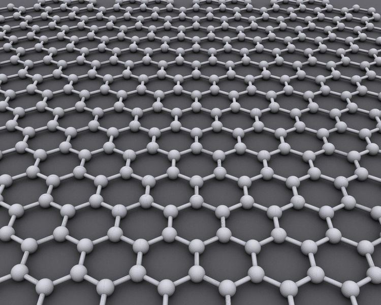
Graphene is a crystalline allotrope of carbon with 2-dimensional properties. Its carbon atoms are densely packed in a regular atomic-scale chicken wire (hexagonal) pattern.
Each atom has four bonds, one σ bond with each of its three neighbors and one π-bond that is oriented out of plane. The atoms are about 1.42 Å apart.
Graphene's hexagonal lattice can be regarded as two interleaving triangular lattices. This perspective was successfully used to calculate the band structure for a single graphite layer using a tight-binding approximation.
Graphene's stability is due to its tightly packed carbon atoms and a sp2 orbital hybridization – a combination of orbitals s, px and py that constitute the σ-bond. The final pz electron makes up the π-bond. The π-bonds hybridize together to form the π-band and π∗-bands. These bands are responsible for most of graphene's notable electronic properties, via the half-filled band that permits free-moving electrons.
Graphene sheets in solid form usually show evidence in diffraction for graphite's (002) layering. This is true of some single-walled nanostructures. However, unlayered graphene with only (hk0) rings has been found in the core of presolar graphite onions. TEM studies show faceting at defects in flat graphene sheets and suggest a role for two-dimensional crystallization from a melt.
Graphene can self-repair holes in its sheets, when exposed to molecules containing carbon, such as hydrocarbons. Bombarded with pure carbon atoms, the atoms perfectly align into hexagons, completely filling the holes.
The atomic structure of isolated, single-layer graphene was studied by TEM on sheets of graphene suspended between bars of a metallic grid. Electron diffraction patterns showed the expected honeycomb lattice. Suspended graphene showed "rippling" of the flat sheet, with amplitude of about one nanometer. These ripples may be intrinsic to the material as a result of the instability of two-dimensional crystals, or may originate from the ubiquitous dirt seen in all TEM images of graphene. Atomic resolution real-space images of isolated, single-layer graphene on SiO
2 substrates are available via scanning tunneling microscopy (STM). Photoresist residue, which must be removed to obtain atomic-resolution images, may be the "adsorbates" observed in TEM images, and may explain the observed rippling. Rippling on SiO
2 is caused by conformation of graphene to the underlying SiO
2 and is not intrinsic.
Chemical
Graphene is the only form of carbon (or solid material) in which every atom is available for chemical reaction from two sides (due to the 2D structure). Atoms at the edges of a graphene sheet have special chemical reactivity. Graphene has the highest ratio of edge atoms of any allotrope. Defects within a sheet increase its chemical reactivity. The onset temperature of reaction between the basal plane of single-layer graphene and oxygen gas is below 260 °C (530 K). Graphene combusts at 350 °C (620 K). Graphene is commonly modified with oxygen- and nitrogen-containing functional groups and analyzed by infrared spectroscopy and X-ray photoelectron spectroscopy. However, determination of structures of graphene with oxygen- and nitrogen- functional groups requires the structures to be well controlled.
Single-layer graphene is a hundred times more chemically reactive than thicker sheets.
Graphene placed on a soda-lime glass (SLG) substrate under ambient conditions exhibited spontaneous n-doping (1.33 × 10¹³ e/cm2) via surface-transfer. On p-type copper indium gallium diselenide (CIGS) semiconductor itself deposited on SLG n-doping reached 2.11 × 10¹³ e/cm2.
Electronic
Graphene is a zero-gap semiconductor, because its conduction and valence bands meet at the Dirac points. The Dirac points are six locations in momentum space, on the edge of the Brillouin zone, divided into two non-equivalent sets of three points. The two sets are labeled K and K'. The sets give graphene a valley degeneracy of gv = 2. By contrast, for traditional semiconductors the primary point of interest is generally Γ, where momentum is zero. Four electronic properties separate it from other condensed matter systems.
However, if the in-plane direction is confined, in which case it is referred to as a nanoribbon, its electronic structure is different. . If it is "zig-zag", the bandgap is zero. If it is "armchair", the bandgap is non-zero (see figure).
Electronic spectrum
Electrons propagating through graphene's honeycomb lattice effectively lose their mass, producing quasi-particles that are described by a 2D analogue of the Dirac equation rather than the Schrödinger equation for spin- 1⁄2 particles.
Dispersion relation
When atoms are placed onto the graphene hexagonal lattice, the overlap between the pz(π) orbitals and the s or the px and py orbitals is zero by symmetry. The pz electrons forming the π bands in graphene can be treated independently. Within this π-band approximation, using a conventional tight-binding model, the dispersion relation (restricted to first-nearest-neighbor interactions only) that produces energy of the electrons with wave vector k is
with the nearest-neighbor (π orbitals) hopping energy γ0 ≈ 6981448609416360000♠2.8 eV and the lattice constant a ≈ 6990246000000000000♠2.46 Å. The conduction and valence bands, respectively, correspond to the different signs. With one pz electron per atom in this model the valence band is fully occupied, while the conduction band is vacant. The two bands touch at the zone corners (the K point in the Brillouin zone), where there is a zero density of states but no band gap. The graphene sheet thus displays a semimetallic (or zero-gap semiconductor) character, although not if rolled into a carbon nanotube, due to its curvature. Two of the six Dirac points are independent, while the rest are equivalent by symmetry. In the vicinity of the K-points the energy depends linearly on the wave vector, similar to a relativistic particle. Since an elementary cell of the lattice has a basis of two atoms, the wave function has an effective 2-spinor structure.
As a consequence, at low energies, even neglecting the true spin, the electrons can be described by an equation that is formally equivalent to the massless Dirac equation. Hence, the electrons and holes are called Dirac fermions. This pseudo-relativistic description is restricted to the chiral limit, i.e., to vanishing rest mass M0, which leads to additional features:
Here vF ~ 7006100000000000000♠106 m/s (.003 c) is the Fermi velocity in graphene, which replaces the velocity of light in the Dirac theory;
The equation describing the electrons' linear dispersion relation is
where the wavevector k is measured from the Dirac points (the zero of energy is chosen here to coincide with the Dirac points). The equation uses a pseudospin matrix formula that describes two sublattices of the honeycomb lattice.
Single-atom wave propagation
Electron waves in graphene propagate within a single-atom layer, making them sensitive to the proximity of other materials such as high-κ dielectrics, superconductors and ferromagnetics.
Electron transport
Graphene displays remarkable electron mobility at room temperature, with reported values in excess of 7004150000000000000♠15000 cm2⋅V−1⋅s−1. Hole and electron mobilities were expected to be nearly identical. The mobility is nearly independent of temperature between 7001100000000000000♠10 K and 7002100000000000000♠100 K, which implies that the dominant scattering mechanism is defect scattering. Scattering by graphene's acoustic phonons intrinsically limits room temperature mobility to 7005200000000000000♠200000 cm2⋅V−1⋅s−1 at a carrier density of 7012100000000000000♠1012 cm−2, 7007100000000000000♠10×106 times greater than copper.
The corresponding resistivity of graphene sheets would be 6994100000000000000♠10−6 Ω⋅cm. This is less than the resistivity of silver, the lowest otherwise known at room temperature. However, on SiO
2 substrates, scattering of electrons by optical phonons of the substrate is a larger effect than scattering by graphene’s own phonons. This limits mobility to 7004400000000000000♠40000 cm2⋅V−1⋅s−1.
Charge transport is affected by adsorption of contaminants such as water and oxygen molecules. This leads to non-repetitive and large hysteresis I-V characteristics. Researchers must carry out electrical measurements in vacuum. Graphene surfaces can be protected by a coating with materials such as SiN, PMMA and h-BN. In January 2015, the first stable graphene device operation in air over several weeks was reported, for graphene whose surface was protected by aluminum oxide. In 2015 lithium-coated graphene was observed to exhibit superconductivity and in 2017 evidence for unconventional superconductivity was demonstrated in single layer graphene placed on the electron-doped (non-chiral) d-wave superconductor Pr2−xCexCuO4 (PCCO).
Electrical resistance in 40-nanometer-wide nanoribbons of epitaxial graphene changes in discrete steps. The ribbons' conductance exceeds predictions by a factor of 10. The ribbons can act more like optical waveguides or quantum dots, allowing electrons to flow smoothly along the ribbon edges. In copper, resistance increases in proportion to length as electrons encounter impurities.
Transport is dominated by two modes. One is ballistic and temperature independent, while the other is thermally activated. Ballistic electrons resemble those in cylindrical carbon nanotubes. At room temperature, resistance increases abruptly at a particular length—the ballistic mode at 16 micrometres and the other at 160 nanometres.
Graphene electrons can cover micrometer distances without scattering, even at room temperature.
Despite zero carrier density near the Dirac points, graphene exhibits a minimum conductivity on the order of
2 substrate may lead to local puddles of carriers that allow conduction. Several theories suggest that the minimum conductivity should be
Near zero carrier density graphene exhibits positive photoconductivity and negative photoconductivity at high carrier density. This is governed by the interplay between photoinduced changes of both the Drude weight and the carrier scattering rate.
Graphene doped with various gaseous species (both acceptors and donors) can be returned to an undoped state by gentle heating in vacuum. Even for dopant concentrations in excess of 1012 cm−2 carrier mobility exhibits no observable change. Graphene doped with potassium in ultra-high vacuum at low temperature can reduce mobility 20-fold. The mobility reduction is reversible on removing the potassium.
Due to graphene's two dimensions, charge fractionalization (where the apparent charge of individual pseudoparticles in low-dimensional systems is less than a single quantum) is thought to occur. It may therefore be a suitable material for constructing quantum computers using anyonic circuits.
Dirac fluid
Charged particles in high-purity graphene behave as a strongly interacting, quasi-relativistic plasma. The particles move in a fluid-like manner, traveling along a single path and interacting with high frequency. The behavior was observed in a graphene sheet faced on both sides with a h-BN crystal sheet.
Anomalous quantum Hall effect
The quantum Hall effect is a quantum mechanical version of the Hall effect, which is the production of transverse (perpendicular to the main current) conductivity in the presence of a magnetic field. The quantization of the Hall effect
Graphene shows the quantum Hall effect with respect to conductivity quantization: the effect is anomalous in that the sequence of steps is shifted by 1/2 with respect to the standard sequence and with an additional factor of 4. Graphene's Hall conductivity is
This behavior is a direct result of graphene's massless Dirac electrons. In a magnetic field, their spectrum has a Landau level with energy precisely at the Dirac point. This level is a consequence of the Atiyah–Singer index theorem and is half-filled in neutral graphene, leading to the "+1/2" in the Hall conductivity. Bilayer graphene also shows the quantum Hall effect, but with only one of the two anomalies (i.e.
Unlike normal metals, graphene's longitudinal resistance shows maxima rather than minima for integral values of the Landau filling factor in measurements of the Shubnikov–de Haas oscillations, whereby the term integral quantum Hall effect. These oscillations show a phase shift of π, known as Berry’s phase. Berry’s phase arises due to the zero effective carrier mass near the Dirac points. The temperature dependence of the oscillations reveals that the carriers have a non-zero cyclotron mass, despite their zero effective mass.
Graphene samples prepared on nickel films, and on both the silicon face and carbon face of silicon carbide, show the anomalous effect directly in electrical measurements. Graphitic layers on the carbon face of silicon carbide show a clear Dirac spectrum in angle-resolved photoemission experiments. The effect is observed in cyclotron resonance and tunneling experiments.
Strong magnetic fields
In magnetic fields above 10 tesla or so additional plateaus of the Hall conductivity at σxy = νe2/h with ν = 0, ±1, ±4 are observed. A plateau at ν = 3 and the fractional quantum Hall effect at ν = 1⁄3 were also reported.
These observations with ν = 0, ±1, ±3, ±4 indicate that the four-fold degeneracy (two valley and two spin degrees of freedom) of the Landau energy levels is partially or completely lifted.
Casimir effect
The Casimir effect is an interaction between disjoint neutral bodies provoked by the fluctuations of the electrodynamical vacuum. Mathematically it can be explained by considering the normal modes of electromagnetic fields, which explicitly depend on the boundary (or matching) conditions on the interacting bodies' surfaces. Since graphene/electromagnetic field interaction is strong for a one-atom-thick material, the Casimir effect is of interest.
Van der Waals force
The Van der Waals force (or dispersion force) is also unusual, obeying an inverse cubic, asymptotic power law in contrast to the usual inverse quartic.
'Massive' electrons
Graphene's unit cell has two identical carbon atoms and two zero-energy states: one in which the electron resides on atom A, the other in which the electron resides on atom B. However, if the two atoms in the unit cell are not identical, the situation changes. Hunt et al. showed that placing hexagonal boron nitride (h-BN) in contact with graphene can alter the potential felt at atom A versus atom B enough that the electrons develop a mass and accompanying band gap of about 30 meV [0.03 Electron Volt(eV)].
The mass can be positive or negative. An arrangement that slightly raises the energy of an electron on atom A relative to atom B gives it a positive mass, while an arrangement that raises the energy of atom B produces a negative electron mass. The two versions behave alike and are indistinguishable via optical spectroscopy. An electron traveling from a positive-mass region to a negative-mass region must cross an intermediate region where its mass once again becomes zero. This region is gapless and therefore metallic. Metallic modes bounding semiconducting regions of opposite-sign mass is a hallmark of a topological phase and display much the same physics as topological insulators.
If the mass in graphene can be controlled, electrons can be confined to massless regions by surrounding them with massive regions, allowing the patterning of quantum dots, wires and other mesoscopic structures. It also produces one-dimensional conductors along the boundary. These wires would be protected against backscattering and could carry currents without dissipation.
Optical
Graphene's unique optical properties produce an unexpectedly high opacity for an atomic monolayer in vacuum, absorbing πα ≈ 2.3% of red light, where α is the fine-structure constant. This is a consequence of the "unusual low-energy electronic structure of monolayer graphene that features electron and hole conical bands meeting each other at the Dirac point... [which] is qualitatively different from more common quadratic massive bands." Based on the Slonczewski–Weiss–McClure (SWMcC) band model of graphite, the interatomic distance, hopping value and frequency cancel when optical conductance is calculated using Fresnel equations in the thin-film limit.
Although confirmed experimentally, the measurement is not precise enough to improve on other techniques for determining the fine-structure constant.
Multi-Parametric Surface Plasmon Resonance was used to characterize both thickness and refractive index of chemical-vapor-deposition (CVD)-grown graphene films. The measured refractive index and extinction coefficient values at 670 nm wavelength are 3.135 and 0.897, respectively. The thickness was determined as 3.7Å from a 0.5mm area, which agrees with 3.35Å reported for layer-to-layer carbon atom distance of graphite crystals.
The method can be used for real-time label-free interactions of graphene with organic and inorganic substances. The existence of unidirectional surface plasmons in the nonreciprocal graphene-based gyrotropic interfaces has been demonstrated theoretically. By efficiently controlling the chemical potential of graphene, the unidirectional working frequency can be continuously tunable from THz to near-infrared and even visible. Particularly, the unidirectional frequency bandwidth can be 1– 2 orders of magnitude larger than that in metal under the same magnetic field, which arises from the superiority of extremely small effective electron mass in graphene.
Graphene's band gap can be tuned from 0 to 6980400544121750000♠0.25 eV (about 5 micrometre wavelength) by applying voltage to a dual-gate bilayer graphene field-effect transistor (FET) at room temperature. The optical response of graphene nanoribbons is tunable into the terahertz regime by an applied magnetic field. Graphene/graphene oxide systems exhibit electrochromic behavior, allowing tuning of both linear and ultrafast optical properties.
A graphene-based Bragg grating (one-dimensional photonic crystal) demonstrated its capability for excitation of surface electromagnetic waves in the periodic structure using a 6993633000000000000♠633 nm He–Ne laser as the light source.
Saturable absorption
Such unique absorption could become saturated when the input optical intensity is above a threshold value. This nonlinear optical behavior is termed saturable absorption and the threshold value is called the saturation fluence. Graphene can be saturated readily under strong excitation over the visible to near-infrared region, due to the universal optical absorption and zero band gap. This has relevance for the mode locking of fiber lasers, where fullband mode locking has been achieved by a graphene-based saturable absorber. Due to this special property, graphene has wide application in ultrafast photonics. The optical response of graphene/graphene oxide layers can be tuned electrically. Saturable absorption in graphene could occur at the Microwave and Terahertz bands, owing to its wideband optical absorption property. The microwave saturable absorption in graphene demonstrates the possibility of graphene microwave and terahertz photonics devices, such as a microwave saturable absorber, modulator, polarizer, microwave signal processing and broad-band wireless access networks.
Nonlinear Kerr effect
Under more intensive laser illumination, graphene could possess a nonlinear phase shift due to the optical nonlinear Kerr effect. Based on a typical open and close aperture z-scan measurement, graphene possesses a nonlinear Kerr coefficient of 6993100000000000000♠10−7 cm2⋅W−1, almost nine orders of magnitude larger than that of bulk dielectrics. This suggests that graphene may be a powerful nonlinear Kerr medium, with the possibility of observing a variety of nonlinear effects, the most important of which is the soliton. Thermal lens spectroscopy can be used for measuring the thermo-optic coefficient of graphene and inspecting its thermal nonlinearity.
Excitonic
First-principle calculations with quasiparticle corrections and many-body effects explore the electronic and optical properties of graphene-based materials. The approach is described as three stages. With GW calculation, the properties of graphene-based materials are accurately investigated, including bulk graphene, nanoribbons, edge and surface functionalized armchair oribbons, hydrogen saturated armchair ribbons, Josephson effect in graphene SNS junctions with single localized defect and armchair ribbon scaling properties.
Stability
Ab initio calculations show that a graphene sheet is thermodynamically unstable if its size is less than about 6992200000000000000♠20 nm ("graphene is the least stable structure until about 6000 atoms") and becomes the most stable fullerene (as within graphite) only for molecules larger than 24,000 atoms.
Thermal conductivity
Thermal transport in graphene is an active area of research, which has attracted attention because of the potential for thermal management applications. Early measurements of the thermal conductivity of suspended graphene reported an exceptionally large thermal conductivity of approximately 7003530000000000000♠5300 W⋅m−1⋅K−1, compared with the thermal conductivity of pyrolytic graphite of approximately 7003200000000000000♠2000 W⋅m−1⋅K−1 at room temperature. However, later studies have questioned whether this ultrahigh value was overestimated, and instead measured thermal conductivities between 7003150000000000000♠1500 – 7003250000000000000♠2500 W⋅m−1⋅K−1 for suspended single layer graphene. The large range can be attributed to large measurement uncertainties as well as variations in the graphene quality and processing conditions. In addition, when single-layer graphene is supported on an amorphous material, the thermal conductivity is reduced to about 7002500000000000000♠500 – 7002600000000000000♠600 W⋅m−1⋅K−1 at room temperature as a result of scattering of graphene lattice waves by the substrate, and can be even lower for few layer graphene encased in amorphous oxide. Likewise, polymeric residue can contribute to a similar decrease for suspended graphene to approximately 7002500000000000000♠500 – 7002600000000000000♠600 W⋅m−1⋅K−1for bilayer graphene.
It has been suggested that the isotopic composition, the ratio of 12C to 13C, has a significant impact on thermal conductivity. For example, isotopically pure 12C graphene has higher thermal conductivity than either a 50:50 isotope ratio or the naturally occurring 99:1 ratio. It can be shown by using the Wiedemann–Franz law, that the thermal conduction is phonon-dominated. However, for a gated graphene strip, an applied gate bias causing a Fermi energy shift much larger than kBT can cause the electronic contribution to increase and dominate over the phonon contribution at low temperatures. The ballistic thermal conductance of graphene is isotropic.
Potential for this high conductivity can be seen by considering graphite, a 3D version of graphene that has basal plane thermal conductivity of over a 7003100000000000000♠1000 W⋅m−1⋅K−1 (comparable to diamond). In graphite, the c-axis (out of plane) thermal conductivity is over a factor of ~100 smaller due to the weak binding forces between basal planes as well as the larger lattice spacing. In addition, the ballistic thermal conductance of graphene gives the lower limit of the ballistic thermal conductances, per unit circumference and length of carbon nanotubes.
Despite its 2-D nature, graphene has 3 acoustic phonon modes. The two in-plane modes (LA, TA) have a linear dispersion relation, while the out of plane mode (ZA) has a quadratic dispersion relation. Due to this, the T2 dependent thermal conductivity contribution of the linear modes is dominated at low temperatures by the T1.5 contribution of the out-of-plane mode. Some graphene phonon bands display negative Grüneisen parameters (GPs). At low temperatures (where most optical modes with positive GPs are still not excited) the contribution from the negative GPs will be dominant and thermal expansion coefficient (which is directly proportional to GPs) negative. The lowest negative GPs correspond to the lowest transverse acoustic ZA modes. Phonon frequencies for such modes increase with the in-plane lattice parameter since atoms in the layer upon stretching will be less free to move in the z direction. This is similar to the behavior of a stretched string that has vibrations of smaller amplitude and higher frequency. This phenomenon, named "membrane effect," was predicted by Lifshitz in 1952.
Melting point
An early prediction suggested a melting point of ~4125 K. Recent, more sophisticated, modelling has increased this temperature to at least 5000 K. At 6000 K (the sun's surface having an effective temperature of 5,777 K) graphene melts into an agglomeration of loosely coupled doubled bonded chains, before becoming a gas.
Mechanical
The carbon–carbon bond length in graphene is about 0.142 nanometers. Graphene sheets stack to form graphite with an interplanar spacing of 6990335000000000000♠0.335 nm.
Graphene is the strongest material ever tested, with an intrinsic tensile strength of 130 GPa and a Young's modulus (stiffness) of 7012100000000000000♠1 TPa (7008150000000000000♠150000000 psi). The Nobel announcement illustrated this by saying that a 1 square meter graphene hammock would support a 7000400000000000000♠4 kg cat but would weigh only as much as one of the cat's whiskers, at 6993769999999999999♠0.77 mg (about 0.001% of the weight of 7000100000000000000♠1 m2 of paper).
Large-angle-bent graphene monolayer has been achieved with negligible strain, showing mechanical robustness of the two-dimensional carbon nanostructure. Even with extreme deformation, excellent carrier mobility in monolayer graphene can be preserved.
The spring constant of suspended graphene sheets has been measured using an atomic force microscope (AFM). Graphene sheets were suspended over SiO
2 cavities where an atomic force microscope (AFM) tip was used to apply a stress to the sheet to test its mechanical properties. Its spring constant was in the range 1–5 N/m and the stiffness was 7011500000000000000♠0.5 TPa, which differs from that of bulk graphite. These intrinsic properties could lead to applications such as NEMS as pressure sensors and resonators. Due to its large surface energy and out of plane ductility, flat graphene sheets are unstable with respect to scrolling, i.e. bending into a cylindrical shape, which is its lower-energy state.
As is true of all materials, regions of graphene are subject to thermal and quantum fluctuations in relative displacement. Although the amplitude of these fluctuations is bounded in 3D structures (even in the limit of infinite size), the Mermin–Wagner theorem shows that the amplitude of long-wavelength fluctuations grows logarithmically with the scale of a 2D structure and would therefore be unbounded in structures of infinite size. Local deformation and elastic strain are negligibly affected by this long-range divergence in relative displacement. It is believed that a sufficiently large 2D structure, in the absence of applied lateral tension, will bend and crumple to form a fluctuating 3D structure. Researchers have observed ripples in suspended layers of graphene. It has been proposed that the ripples are caused by thermal fluctuations in the material. As a consequence of these dynamical deformations, it is debatable whether graphene is truly a 2D structure. It has recently been shown that these ripples, if amplified through the introduction of vacancy defects, can impart a negative Poisson's ratio into graphene, resulting in the thinnest auxetic material known.
Graphene nanosheets can be incorporated into a nickel matrix through a plating process to form Ni-graphene composites on a target substrate. The enhancement in mechanical properties of the composites is attributed to the high interaction between Ni and graphene and the prevention of the dislocation sliding in the Ni matrix by the graphene.
Fracture toughness
In 2014, researchers indicated that despite its strength, graphene is also relatively brittle, with a fracture toughness of about 4 MPa√m. This indicates that imperfect graphene is likely to crack in a brittle manner like ceramic materials, as opposed to many metallic materials that have fracture toughnesses in the range of 15–50 MPa√m. Later in 2014, the researchers announced that graphene showed a greater ability to distribute force from an impact than any known material, ten times that of steel per unit weight. The force was transmitted at 22.2 kilometres per second (13.8 mi/s).
Spin transport
Graphene is claimed to be an ideal material for spintronics due to its small spin-orbit interaction and the near absence of nuclear magnetic moments in carbon (as well as a weak hyperfine interaction). Electrical spin current injection and detection has been demonstrated up to room temperature. Spin coherence length above 1 micrometre at room temperature was observed, and control of the spin current polarity with an electrical gate was observed at low temperature.
Strong magnetic fields
In magnetic fields of ~10 tesla, additional plateaus of Hall conductivity at
These observations with
Spintronic and magnetic properties can be present in graphene simultaneously. Low-defect graphene nanomeshes manufactured using a non-lithographic method exhibit large-amplitude ferromagnetism even at room temperature. Additionally a spin pumping effect is found for fields applied in parallel with the planes of few-layer ferromagnetic nanomeshes, while a magnetoresistance hysteresis loop is observed under perpendicular fields.
Magnetic
In 2014 researchers magnetized graphene by placing it on an atomically smooth layer of magnetic yttrium iron garnet. The graphene's electronic properties were unaffected. Prior approaches involved doping. The dopant's presence negatively affected its electronic properties.
Biological
Researchers in 2011 discovered the ability of graphene to accelerate the osteogenic differentiation of human mesenchymal stem cells without the use of biochemical inducers.
In 2015 researchers used graphene to create biosensors with epitaxial graphene on silicon carbide. The sensors bind to 8-hydroxydeoxyguanosine (8-OHdG) and is capable of selective binding with antibodies. The presence of 8-OHdG in blood, urine and saliva is commonly associated with DNA damage. Elevated levels of 8-OHdG have been linked to increased risk of several cancers.
In 2016 researchers revealed that uncoated graphene can be used as neuro-interface electrode without altering or damaging properties such as signal strength or formation of scar tissue. Graphene electrodes in the body stay significantly more stable than electrodes of tungsten or silicon because of properties such as flexibility, bio-compatibility and conductivity.
Substrate
The electronic properties of graphene are significantly influenced by the supporting substrate. The Si(100)/H surface does not perturb graphene's electronic properties, whereas the interaction between it and the clean Si(100) surface changes its electronic states significantly. This effect results from the covalent bonding between C and surface Si atoms, modifying the π-orbital network of the graphene layer. The local density of states shows that the bonded C and Si surface states are highly disturbed near the Fermi energy.
Monolayer sheets
In 2013 researchers developed a production unit that produces continuous monolayer sheets of high-strength monolayer graphene (HSMG). The process is based on graphene growth on a liquid metal matrix.
Bilayer
Bilayer graphene displays the anomalous quantum Hall effect, a tunable band gap and potential for excitonic condensation. Bilayer graphene typically can be found either in twisted configurations where the two layers are rotated relative to each other or graphitic Bernal stacked configurations where half the atoms in one layer lie atop half the atoms in the other. Stacking order and orientation govern its optical and electronic properties.
One synthesis method is chemical vapor deposition, which can produce large bilayer regions that almost exclusively conform to a Bernal stack geometry.
Superlattices
Periodically stacked graphene and its insulating isomorph provide a fascinating structural element in implementing highly functional superlattices at the atomic scale, which offers possibilities in designing nanoelectronic and photonic devices. Various types of superlattices can be obtained by stacking graphene and its related forms. The energy band in layer-stacked superlattices is more sensitive to the barrier width than that in conventional III–V semiconductor superlattices. When adding more than one atomic layer to the barrier in each period, the coupling of electronic wavefunctions in neighboring potential wells can be significantly reduced, which leads to the degeneration of continuous subbands into quantized energy levels. When varying the well width, the energy levels in the potential wells along the L-M direction behave distinctly from those along the K-H direction.
Nanoribbons
Graphene nanoribbons ("nanostripes" in the "zig-zag" orientation), at low temperatures, show spin-polarized metallic edge currents, which suggest spintronics applications. (In the "armchair" orientation, the edges behave like semiconductors.)
Quantum dots
Several techniques can prepare nanostructured graphene, e.g., graphene quantum dots (GQDs); these techniques mainly include electron beam lithography, chemical synthesis, electrochemical preparation, graphene oxide (GO) reduction, C60 catalytic transformation, the microwave assisted hydrothermal method (MAH), the Soft-Template method, the hydrothermal method, and the ultrasonic exfoliation method.
Oxide
Using paper-making techniques on dispersed, oxidized and chemically processed graphite in water, monolayer flakes form a single sheet and create strong bonds. These sheets, called graphene oxide paper, have a measured tensile modulus of 32 GPa. The chemical property of graphite oxide is related to the functional groups attached to graphene sheets. These can change the polymerization pathway and similar chemical processes. Graphene oxide flakes in polymers display enhanced photo-conducting properties. Graphene is normally hydrophobic and impermeable to all gases and liquids (vacuum-tight). However, when formed into graphene oxide-based capillary membrane, both liquid water and water vapor flow through as quickly as if the membrane was not present.
Chemical modification
Soluble fragments of graphene can be prepared in the laboratory through chemical modification of graphite. First, microcrystalline graphite is treated with an acidic mixture of sulfuric acid and nitric acid. A series of oxidation and exfoliation steps produce small graphene plates with carboxyl groups at their edges. These are converted to acid chloride groups by treatment with thionyl chloride; next, they are converted to the corresponding graphene amide via treatment with octadecylamine. The resulting material (circular graphene layers of 5.3 angstrom thickness) is soluble in tetrahydrofuran, tetrachloromethane and dichloroethane.
Refluxing single-layer graphene oxide (SLGO) in solvents leads to size reduction and folding of individual sheets as well as loss of carboxylic group functionality, by up to 20%, indicating thermal instabilities of SLGO sheets dependent on their preparation methodology. When using thionyl chloride, acyl chloride groups result, which can then form aliphatic and aromatic amides with a reactivity conversion of around 70–80%.
Hydrazine reflux is commonly used for reducing SLGO to SLG(R), but titrations show that only around 20–30% of the carboxylic groups are lost, leaving a significant number available for chemical attachment. Analysis of such SLG(R) reveals that the system is unstable. Using a room temperature stirring with HCl (< 1.0 M) leads to around 60% loss of COOH functionality. Room temperature treatment of SLGO with carbodiimides leads to the collapse of the individual sheets into star-like clusters that exhibited poor subsequent reactivity with amines (c. 3–5% conversion of the intermediate to the final amide). It is apparent that conventional chemical treatment of carboxylic groups on SLGO generates morphological changes of individual sheets that leads to a reduction in chemical reactivity, which may potentially limit their use in composite synthesis. Therefore, chemical reactions types have been explored. SLGO has also been grafted with polyallylamine, cross-linked through epoxy groups. When filtered into graphene oxide paper, these composites exhibit increased stiffness and strength relative to unmodified graphene oxide paper.
Full hydrogenation from both sides of graphene sheet results in graphane, but partial hydrogenation leads to hydrogenated graphene. Similarly, both-side fluorination of graphene (or chemical and mechanical exfoliation of graphite fluoride) leads to fluorographene (graphene fluoride), while partial fluorination (generally halogenation) provides fluorinated (halogenated) graphene.
Ligand/complex
Graphene can be a ligand to coordinate metals and metal ions by introducing functional groups. Structures of graphene ligands are similar to e.g. metal-porphyrin complex, metal-phthalocyanine complex and metal-phenanthroline complex. Copper and nickel ions can be coordinated with graphene ligands.
Fiber
In 2011, researchers reported making fibers using chemical vapor deposition grown graphene films. The method was scalable and controllable, delivering tunable morphology and pore structure by controlling the evaporation of solvents with suitable surface tension. Flexible all-solid-state supercapacitors based on such fibers were demonstrated in 2013.
In 2015 intercalating small graphene fragments into the gaps formed by larger, coiled graphene sheets after annealing provided pathways for conduction, while the fragments helped reinforce the fibers. The resulting fibers offered better thermal and electrical conductivity and mechanical strength. Thermal conductivity reached 1290 watts per meter per kelvin, while tensile strength reached 1080 megapascals.
In 2016, kilometer-scale continuous graphene fibers with outstanding mechanical properties and excellent electrical conductivity were produced by high-throughput wet-spinning of graphene oxide liquid crystals followed by graphitization through a full-scale synergetic defect-engineering strategy.
3D
In 2013, a three-dimensional honeycomb of hexagonally arranged carbon was termed 3D graphene. Self-supporting 3D graphene was produced that year. Researchers at Stony Brook University have reported a novel radical-initiated crosslinking method to fabricate porous 3D free-standing architectures of graphene and carbon nanotubes using nanomaterials as building blocks without any polymer matrix as support. 3D structures can be fabricated by using either CVD or solution-based methods. A 2016 review summarized the techniques for fabrication of 3D graphene and other related two-dimensional materials. These 3D graphene (all-carbon) scaffolds/foams have potential applications in fields such as energy storage, filtration, thermal management and biomedical devices and implants.
In 2016 box-shaped graphene (BSG) nanostructure resulted from mechanical cleavage of pyrolytic graphite. The discovered nanostructure is a multilayer system of parallel hollow nanochannels located along the surface that displayed quadrangular cross-section. The thickness of the channel walls is approximately equal to 1 nm. Potential applications include: ultra-sensitive detectors, high-performance catalytic cells, nanochannels for DNA sequencing and manipulation, high-performance heat sinking surfaces, rechargeable batteries of enhanced performance, nanomechanical resonators, electron multiplication channels in emission nanoelectronic devices, high-capacity sorbents for safe hydrogen storage.
Three dimensional bilayer graphene was reported in 2012 and 2014.
Gyroid
In 2017 researchers created a graphene gyroid that has five percent of the density of steel, yet is ten times as strong with an enormous surface area to volume ratio. They compressed heated graphene flakes. They then constructed high resolution 3D-printed models of plastic of various configurations – similar to the gyroids that graphene form naturally, though thousands of times larger. These shapes were then tested for tensile strength and compression, and compared to the computer simulations. When then graphene was swapped out for polymers or metals, similar gains in strength were seen.
Molded
A film of graphene soaked in solvent to make it swell and become malleable was overlaid on an underlying substrate "former". The solvent evaporated, leaving behind a layer of graphene that had taken on the shape of the underlying structure. In this way the team was able to produce a range of relatively intricate micro-structured shapes. Features vary from 3.5 to 50 μm. Pure graphene and gold-decorated graphene were each successfully integrated with the substrate.
Aerogel
An aerogel made of graphene layers separated by carbon nanotubes was measured at 0.16 milligrams per cubic centimeter. A solution of graphene and carbon nanotubes in a mold is freeze dried to dehydrate the solution, leaving the aerogel. The material has superior elasticity and absorption. It can recover completely after more than 90% compression, and absorb up to 900 times its weight in oil, at a rate of 68.8 grams per second.
Pillared
Pillared graphene is a hybrid carbon structure consisting of an oriented array of carbon nanotubes connected at each end to a graphene sheet. It was first described theoretically in 2008. Pillared graphene has not been synthesized in the laboratory.
Reinforced
Graphene sheets reinforced with embedded carbon nanotubes ("rebar") are easier to manipulate, while improving the electrical and mechanical qualities of both materials.
Functionalized single- or multiwalled carbon nanotubes are spin-coated on copper foils and then heated and cooled, using the nanotubes as the carbon source. Under heating, the functional carbon groups decompose into graphene, while the nanotubes partially split and form in-plane covalent bonds with the graphene, adding strength. π–π stacking domains add more strength. The nanotubes can overlap, making the material a better conductor than standard CVD-grown graphene. The nanotubes effectively bridge the grain boundaries found in conventional graphene. The technique eliminates the traces of substrate on which later-separated sheets were deposited using epitaxy.
Stacks of a few layers have been proposed as a cost-effective and physically flexible replacement for indium tin oxide (ITO) used in displays and photovoltaic cells.
Nanocoil
In 2015 a coiled form of graphene was discovered in graphitic carbon (coal). The spiraling effect is produced by defects in the material's hexagonal grid that causes it to spiral along its edge, mimicking a Riemann surface, with the graphene surface approximately perpendicular to the axis. When voltage is applied to such a coil, current flows around the spiral, producing a magnetic field. The phenomenon applies to spirals with either zigzag or armchair orientations, although with different current distributions. Computer simulations indicated that a conventional spiral inductor of 205 microns in diameter could be matched by a nanocoil just 70 nanometers wide, with a field strength reaching as much as 1 tesla, about the same as the coils found in typical loudspeakers, about the same field strength as some MRI machines. They found the magnetic field would be strongest in the hollow, nanometer-wide cavity at the spiral's center.
A solenoid made with such a coil behaves as a quantum conductor whose current distribution between the core and exterior varies with applied voltage, resulting in nonlinear inductance.
Production
Multiple production techniques have been developed. Isolated 2D crystals cannot be grown via chemical synthesis beyond small sizes even in principle, because the rapid growth of phonon density with increasing lateral size forces 2D crystallites to bend into the third dimension. In all cases, graphene must bond to a substrate to retain its two-dimensional shape.
Exfoliation
As of 2014, exfoliation produced graphene with the lowest number of defects and highest electron mobility.
Geim and Novoselov initially used adhesive tape to pull graphene sheets away from graphite. Achieving single layers typically requires multiple exfoliation steps. After exfoliation the flakes are deposited on a silicon wafer. Crystallites larger than 1 mm and visible to the naked eye can be obtained.
Alternatively a sharp single-crystal diamond wedge cleave layers from a graphite source.
Rapid heating of graphite oxide and exfoliation yields highly dispersed carbon powder with a few percent of graphene flakes.
Another method is reduction of graphite oxide monolayer films, e.g. by hydrazine with annealing in argon/hydrogen with an almost intact carbon framework that allows efficient removal of functional groups. Measured charge carrier mobility exceeded 1,000 centimetres (393.70 in)/Vs.
Defect-free, unoxidized graphene-containing liquids can be made from graphite using mixers that produce local shear rates greater than 7005100000000000000♠10×104.
Burning a graphite oxide coated DVD produced a conductive graphene film (1738 siemens per meter) and specific surface area (1520 square meters per gram) that was highly resistant and malleable.
With definite cleavage parameters, box-shaped graphene (BSG) nanostructure can be prepared on graphite crystal.
Sonication
Dispersing graphite in a liquid medium can produce graphene by sonication followed by centrifugation, producing concentrations of 7000210000000000000♠2.1 mg/mL in N-methylpyrrolidone. Using a suitable ionic liquid as the dispersing liquid medium produced concentrations of 7000533000000000000♠5.33 mg/mL. Restacking is an issue with this technique. Adding a surfactant to a solvent prior to sonication prevents restacking by adsorbing to the graphene's surface. This produces a higher graphene concentration, but removing the surfactant requires chemical treatments.
Sonicating graphite at the interface of two immiscible liquids, most notably heptane and water, produced macro-scale graphene films. The graphene sheets are adsorbed to the high energy interface between the materials and are kept from restacking. The sheets are up to about 95% transparent and conductive.
Molten salts
Graphite particles can be corroded in molten salts to form a variety of carbon nanostructures including graphene. Hydrogen cations, dissolved in molten lithium chloride, can be discharged on cathodically polarized graphite rods, which then intercalate, peeling graphene sheets. The graphene nanosheets produced displayed a single-crystalline structure with a lateral size of several hundred nanometers and a high degree of crystallinity and thermal stability.
Electrochemical synthesis
Electrochemical synthesis can exfoliate graphene. Varying a pulsed voltage controls thickness, flake area, number of defects and affects its properties. The process begins by bathing the graphite in a solvent for intercalation. The process can be tracked by monitoring the solution’s transparency with an LED and photodiode.
Hydrothermal self-assembly
Graphene has been prepared by using a sugar (e.g. glucose, sugar, fructose, etc.) This substrate-free "bottom-up" synthesis is safer, simpler and more environmentally friendly than exfoliation. The method can control thickness, ranging from monolayer to multilayers, which is known as "Tang-Lau Method".
Epitaxy
Epitaxial graphene may be coupled to surfaces weakly enough (by Van der Waals forces) to retain the two dimensional electronic band structure of isolated graphene.
Heating silicon carbide (SiC) to high temperatures (7003137315000000000♠1100 °C) under low pressures (c. 10−6 torr) reduces it to graphene.
A normal silicon wafer coated with a layer of germanium (Ge) dipped in dilute hydrofluoric acid strips the naturally forming germanium oxide groups, creating hydrogen-terminated germanium. CVD can coat that with graphene.
A two-step CVD process is shown to grow graphene directly on TiO2 crystals or exfoliated TiO2 nanosheets without using a metal catalyst.
Metal substrates
The atomic structure of metal substrates including ruthenium, iridium, nickel and copper has been used as substrates for graphene production. In 2015 researchers announced the use of commercial copper foils for graphene production, reducing substrate costs by 100-fold.
Sodium ethoxide pyrolysis
Gram quantities were produced by the reduction of ethanol by sodium metal, followed by pyrolysis and washing with water.
Roll-to-roll
In 2014 a two-step roll-to-roll manufacturing process was announced. The first roll-to-roll step produces the graphene via chemical vapor deposition. The second step binds the graphene to a substrate.
Cold wall
Growing graphene in an industrial resistive-heating cold wall CVD system was claimed to produce graphene 100 times faster than conventional CVD systems, cut costs by 99% and produce material with enhanced electronic qualities. Cold wall CVD technique can be used to study the underlying surface science involved in graphene nucleation and growth as it allows control of process parameters like gas flow rates, temperature and pressure. A home-built vertical cold wall system used resistive heating by passing direct current through the substrate. It provided insight into a typical surface-mediated nucleation and growth mechanism involved in two-dimensional materials grown using catalytic CVD under conditions sought out in the semiconductor industry.
Wafer scale CVD
CVD graphene is scalable and has been integrated with ubiquitous CMOS technology via growth on deposited copper thin film catalyst on 100 to 300 mm standard Si/SiO2 wafers on an Axitron Black Magic system. Monolayer graphene coverage of >95% is achieved on 100 to 300 mm wafer substrates with negligible defects, confirmed by extensive Raman mapping.
Nanotube slicing
Graphene can be created by opening carbon nanotubes by cutting or etching. In one such method multi-walled carbon nanotubes are cut open in solution by action of potassium permanganate and sulfuric acid.
Carbon dioxide reduction
A highly exothermic reaction combusts magnesium in an oxidation–reduction reaction with carbon dioxide, producing carbon nanoparticles including graphene and fullerenes.
Spin coating
In 2014, carbon nanotube-reinforced graphene was made via spin coating and annealing functionalized carbon nanotubes.
Supersonic spray
Supersonic acceleration of droplets through a Laval nozzle was used to deposit reduced graphene-oxide on a substrate. The energy of the impact rearranges the carbon atoms into flawless graphene.
Another approach sprays buckyballs at supersonic speeds onto a substrate. The balls cracked open upon impact and the resulting unzipped cages then bond together to form a graphene film.
Laser
A CO
2 infrared laser produced and patterned porous three-dimensional graphene film networks from commercial polymer films. The result exhibits high electrical conductivity.
Microwave-assisted oxidation
Microwave energy was reported to directly synthesize graphene in one step. This approach avoids use of potassium permanganate in the reaction mixture. MMicrowave radiation assistance allows graphene oxide with or without holes can be synthesized by controlling microwave time. Microwave heating can dramatically shorten the reaction time from days to seconds.
Ion implantation
Accelerating carbon ions under an electrical field into a semiconductor made of thin nickel films on a substrate of SiO2/Si, creates a wafer-scale (4 inches (100 mm)) wrinkle/tear/residue-free graphene layer at a relatively low temperature of 500 °C.
Heated vegetable oil
Researchers heated soybean oil in a furnace for ~30 minutes. The heat decomposed the oil into elemental carbon that deposited on nickel foil as single/few-layer graphene.
Analogs
Analogs (also referred to as "artificial graphene") are two-dimensional systems that exhibit similar properties to graphene. Analogs can be systems in which the physics is easier to observe and to manipulate. In those systems, electrons are not always the chosen particles. They might be optical photons, microwave photons, plasmons, microcavity polaritons or even atoms. Also, the honeycomb structure in which those particles evolve can be of a different nature than carbon atoms in graphene. It can be, respectively, a photonic crystal, an array of metallic rods, metallic nanoparticles, a lattice of coupled microcavities or an optical lattice.
Applications
Graphene is a transparent and flexible conductor that holds great promise for various material/device applications, including solar cells, light-emitting diodes (LED), touch panels and smart windows or phones. China-based 2D Carbon Graphene Material Co.,Ltd, graphene-based touch panel modules have been sold in volume to cell phone, wearable device and home appliance manufacturers. For instance, smart phone products with graphene touch screens are already on the market.
As of 2015 one product was available for commercial use: a graphene-infused printer powder.
In 2016, researchers made a graphene film that can absorb 95% of light incident on it. BAC's 2016 Mono model is said to be made out of graphene as a first of both a street-legal track car and a production car.
Graphene is often produced as a powder and as a dispersion in a polymer matrix. This dispersion is supposedly suitable for advanced composites, paints and coatings, lubricants, oils and functional fluids, capacitors and batteries, thermal management applications, display materials and packaging, solar cells, inks and 3D-printers’ materials and barriers and films. Many other uses for graphene have been proposed or are under development, in areas including electronics, biological engineering, filtration, lightweight/strong composite materials, photovoltaics and energy storage.
Health risks
The toxicity of graphene has been extensively debated in the literature. The most comprehensive review on graphene toxicity summarized the in vitro, in vivo, antimicrobial and environmental effects and highlights the various mechanisms of graphene toxicity. The toxicity of graphene is dependent on factors such as shape, size, purity, post-production processing steps, oxidative state, functional groups, dispersion state, synthesis methods, route, dose of administration and exposure times.
Graphene nanoribbons, graphene nanoplatelets and graphene nano–onions are non-toxic at concentrations up to 50 µg/ml. These nanoparticles do not alter the differentiation of human bone marrow stem cells towards osteoblasts (bone) or adipocytes (fat) suggesting that at low doses graphene nanoparticles are safe for biomedical applications. 10 µm few-layered graphene flakes were able to pierce cell membranes in solution. They were observed to enter initially via sharp and jagged points, allowing graphene to be enter the cell. The physiological effects of this remain uncertain, and this remains a relatively unexplored field.