
 | ||
Vladimir falko electronic properties of bilayer graphene from high to low energies
Bilayer graphene is a material consisting of two layers of graphene. One of the first reports of bilayer graphene was in the seminal 2004 Science paper by Geim and colleagues, in which they described devices "which contained just one, two, or three atomic layers"
Contents
- Vladimir falko electronic properties of bilayer graphene from high to low energies
- How bilayer graphene got a bandgap
- Structure
- Synthesis
- Tunable bandgap
- Emergent complex states
- Excitonic Condensation
- Bilayer Graphene FETs
- Porous Nanoflakes
- Characterisation Technique
- Three dimensional bilayer graphene
- References
How bilayer graphene got a bandgap
Structure
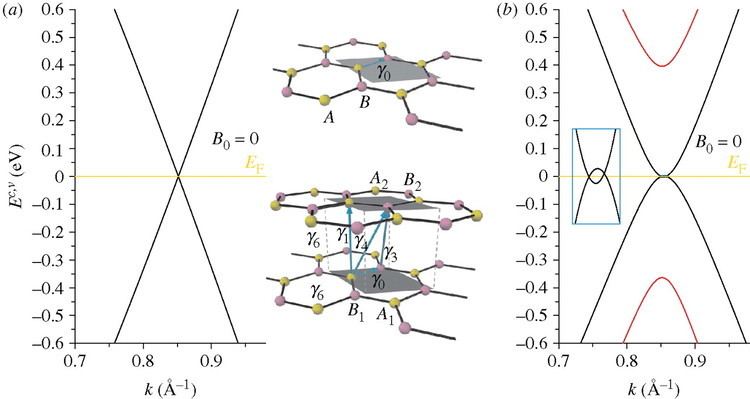
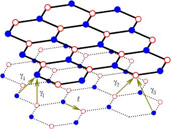
Bilayer graphene can exist in the AB, or Bernal-stacked form, where half of the atoms lie directly over the center of a hexagon in the lower graphene sheet, and half of the atoms lie over an atom, or, less commonly, in the AA form, in which the layers are exactly aligned. In Bernal stacked graphene, twin boundaries are common; transitioning from AB to BA stacking. Twisted layers, where one layer is rotated relative to the other has also been observed.
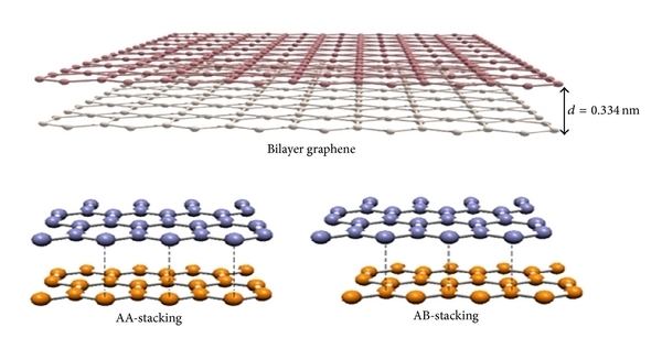
Quantum Monte Carlo methods have been used to calculate the binding energies of AA- and AB-stacked bilayer graphene, which are 11.5(9) and 17.7(9) meV per atom, respectively. This is consistent with the observation that the AB-stacked structure is more stable than the AA-stacked structure.
Synthesis
Bilayer graphene can be made by exfoliation from graphite or by chemical vapor deposition (CVD). In 2016, Rodney S. Ruoff and colleagues showed that large single-crystal bilayer graphene could be produced by oxygen-activated chemical vapour deposition. Later in the same year a Korean group reported the synthesis of wafer-scale single-crystal AB-stacked bilayer graphene
Tunable bandgap
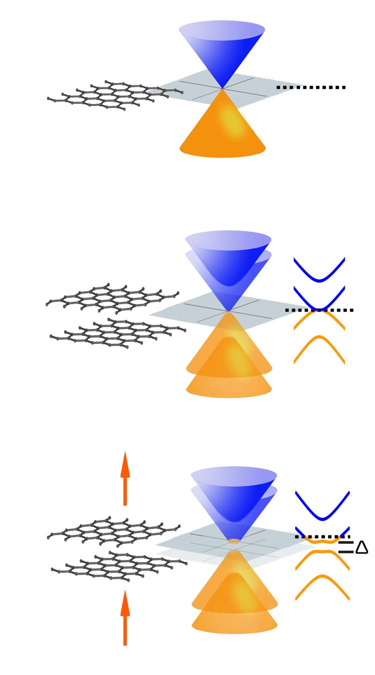
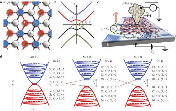
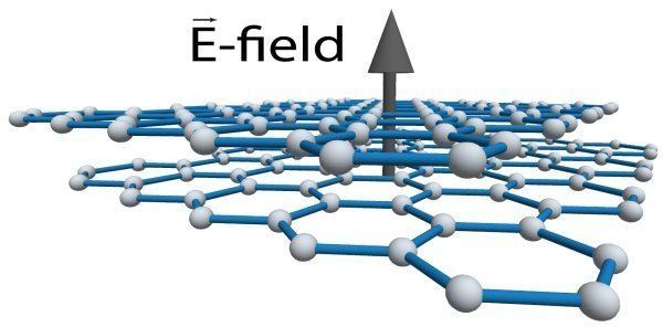
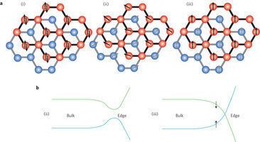
Like monolayer graphene, bilayer graphene has a zero bandgap and thus behaves like a semimetal. In 2007, Allan H. MacDonald and colleagues predicted that a bandgap could be introduced if an electric displacement field were applied to the two layers: a so-called tunable band gap. An experimental demonstration of a tunable bandgap in bilayer graphene was given by Alex Zettl and co-workers in 2009. In 2015 the same group observed 1D ballistic electron conducting channels at bilayer graphene domain walls. A group led by Taisuke Ohta, Lawrence Berkeley National Laboratory, showed that the band gap of bilayer graphene films on silicon carbide could be controlled by selectively adjusting the carrier concentration
Emergent complex states
A trio of papers published in Science in July 2014 described the emergence of complex electronic states in bilayer graphene, notably the fractional quantum Hall effect and showed that this could be tuned by an electric field.
Excitonic Condensation
Bilayer graphene is being studied for its potential to realize a Bose–Einstein condensate of excitons. Electrons and holes are fermions, but when they form an exciton, they become bosons, allowing Bose-Einstein condensation to occur. Exciton condensates in bilayer systems have been shown theoretically to carry a large current.
Bilayer Graphene FETs
Bilayer graphene can be used to construct field effect transistors.
Porous Nanoflakes
Hybridization processes change the intrinsic properties of graphene and/or induce poor interfaces. In 2014 a general route to obtain unstacked graphene via facile, templated, catalytic growth was announced. The resulting material offers specific surface area of 1628 m2 g-1, electrical conductivity and mesoporous structure.
The material is made with a mesoporous nanoflake template. Graphene layers are deposited onto the template. The carbon atoms accumulate in the mesopores, forming protuberances that act as spacers to prevent stacking. Protuberance density is approximately 7014580000000000000♠5.8×10¹⁴ m−2. Graphene is deposited on both sides of the flakes.
During CVD synthesis the protuberances produce intrinsically unstacked double-layer graphene after the removal of the nanoflakes. The presence of such protuberances on the surface can weaken the π-π interactions between graphene layers and thus reduce stacking. The bilayer graphene shows a specific surface area of 7006162800000000000♠1628 m2/g, a pore size ranging from 2 to 7 nm and a total pore volume of 6997200000000000000♠2.0 cm3/g.
Using bilary graphene as cathode material for a lithium sulfur battery yielded reversible capacities of 1034 and 734 mA h/g at discharge rates of 5 and 10 C, respectively. After 1000 cycles reversible capacities of some 530 and 380 mA h/g were retained at 5 and 10 C, with coulombic efficiency constants at 96 and 98%, respectively.
Electrical conductivity of 438 S/cm was obtained. Even after the infiltration of sulfur, electrical conductivity of 107 S cm/1 was retained. The graphene's unique porous structure allowed the effective storage of sulfur in the interlayer space, which gives rise to an efficient connection between the sulfur and graphene and prevents the diffusion of polysulfides into the electrolyte.
Characterisation Technique
Bilayer graphene is difficult to produce. Most of the time there will be contamination from monolayer graphene. Hyperspectral global Raman imaging is an accurate and rapid technique to spatially characterize the quality of the growth. The vibrational modes of a system are its fingerprint, they provide information on the stoichiometry, composition, morphology, stress, number of layers, etc. Monitoring graphene's G and D peaks (around 1580 and 1360 cm−1) intensity gives direct information on the number of layers of the sample.
"Three dimensional bilayer graphene"
A new form of carbon, named "three dimensional bilayer graphene" has been reported. This can be produced by the passage of an electric current through graphite. It consists of hollow, three-dimensional shells bounded by bilayer graphene. Bilayer nanotubes and nanoparticles are often found supported on the graphene shells, and nanotubes seamlessly joined to the shells are also seen.