
 | ||
The term high-κ dielectric refers to a material with a high dielectric constant κ (as compared to silicon dioxide). High-κ dielectrics are used in semiconductor manufacturing processes where they are usually used to replace a silicon dioxide gate dielectric or another dielectric layer of a device. The implementation of high-κ gate dielectrics is one of several strategies developed to allow further miniaturization of microelectronic components, colloquially referred to as extending Moore's Law.
Contents
- Need for high materials
- First principles
- Gate capacitance impact on drive current
- Materials and considerations
- Use in industry
- References
Sometimes these materials are called "high-k" instead of "high-κ" (high kappa).
Need for high-κ materials
Silicon dioxide (SiO2) has been used as a gate oxide material for decades. As transistors have decreased in size, the thickness of the silicon dioxide gate dielectric has steadily decreased to increase the gate capacitance and thereby drive current, raising device performance. As the thickness scales below 2 nm, leakage currents due to tunneling increase drastically, leading to high power consumption and reduced device reliability. Replacing the silicon dioxide gate dielectric with a high-κ material allows increased gate capacitance without the associated leakage effects.
First principles
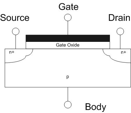
The gate oxide in a MOSFET can be modeled as a parallel plate capacitor. Ignoring quantum mechanical and depletion effects from the Si substrate and gate, the capacitance C of this parallel plate capacitor is given by
Where
Since leakage limitation constrains further reduction of t, an alternative method to increase gate capacitance is alter κ by replacing silicon dioxide with a high-κ material. In such a scenario, a thicker gate oxide layer might be used which can reduce the leakage current flowing through the structure as well as improving the gate dielectric reliability.
Gate capacitance impact on drive current
The drain current ID for a MOSFET can be written (using the gradual channel approximation) as
Where
The term VG − Vth is limited in range due to reliability and room temperature operation constraints, since a too large VG would create an undesirable, high electric field across the oxide. Furthermore, Vth cannot easily be reduced below about 200 mV, because leakage currents due to increased oxide leakage (that is, assuming high-κ dielectrics are not available) and subthreshold conduction raise stand-by power consumption to unacceptable levels. (See the industry roadmap, which limits threshold to 200 mV, and Roy et al. ). Thus, according to this simplified list of factors, an increased ID,sat requires a reduction in the channel length or an increase in the gate dielectric capacitance.
Materials and considerations
Replacing the silicon dioxide gate dielectric with another material adds complexity to the manufacturing process. Silicon dioxide can be formed by oxidizing the underlying silicon, ensuring a uniform, conformal oxide and high interface quality. As a consequence, development efforts have focused on finding a material with a requisitely high dielectric constant that can be easily integrated into a manufacturing process. Other key considerations include band alignment to silicon (which may alter leakage current), film morphology, thermal stability, maintenance of a high mobility of charge carriers in the channel and minimization of electrical defects in the film/interface. Materials which have received considerable attention are hafnium silicate, zirconium silicate, hafnium dioxide and zirconium dioxide, typically deposited using atomic layer deposition.
It is expected that defect states in the high-k dielectric can influence its electrical properties. Defect states can be measured for example by using zero-bias thermally stimulated current, zero-temperature-gradient zero-bias thermally stimulated current spectroscopy, or inelastic electron tunneling spectroscopy (IETS).
Use in industry
The industry has employed oxynitride gate dielectrics since the 1990s, wherein a conventionally formed silicon oxide dielectric is infused with a small amount of nitrogen. The nitride content subtly raises the dielectric constant and is thought to offer other advantages, such as resistance against dopant diffusion through the gate dielectric.
In early 2007, Intel announced the deployment of hafnium-based high-k dielectrics in conjunction with a metallic gate for components built on 45 nanometer technologies, and has shipped it in the 2007 processor series codenamed Penryn. At the same time, IBM announced plans to transition to high-k materials, also hafnium-based, for some products in 2008. While not identified, the most likely dielectric used in such applications are some form of nitrided hafnium silicates (HfSiON). HfO2 and HfSiO are susceptible to crystallization during dopant activation annealing. NEC Electronics has also announced the use of a HfSiON dielectric in their 55 nm UltimateLowPower technology. However, even HfSiON is susceptible to trap-related leakage currents, which tend to increase with stress over device lifetime. This leakage effect becomes more severe as hafnium concentration increases. There is no guarantee however, that hafnium will serve as a de facto basis for future high-k dielectrics. The 2006 ITRS roadmap predicted the implementation of high-k materials to be commonplace in the industry by 2010.