
Density 5.32 g/cm³ Molar mass 144.645 g/mol | Formula GaAs Melting point 1,238 °C | |
 | ||
Appearance Very dark red, vitreous crystals | ||
Gallium arsenide
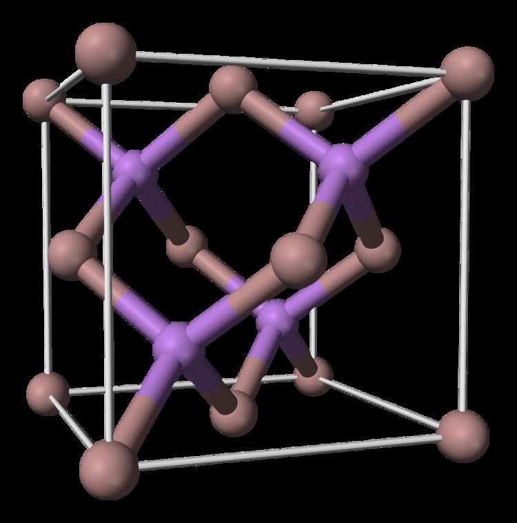
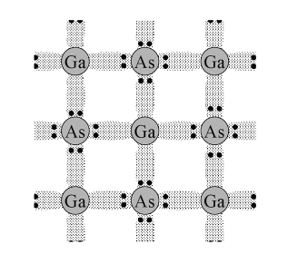
Gallium arsenide (GaAs) is a compound of the elements gallium and arsenic. It is a III-V direct bandgap semiconductor with a zinc blende crystal structure.
Contents
- Gallium arsenide
- Preparation and chemistry
- Semi insulating crystals
- Etching
- GaAs digital logic
- GaAs advantages
- Silicon advantages
- Solar cells and detectors
- Light emission devices
- Fiber optic temperature measurement
- Spin charge converters
- Safety
- References
Gallium arsenide is used in the manufacture of devices such as microwave frequency integrated circuits, monolithic microwave integrated circuits, infrared light-emitting diodes, laser diodes, solar cells and optical windows.
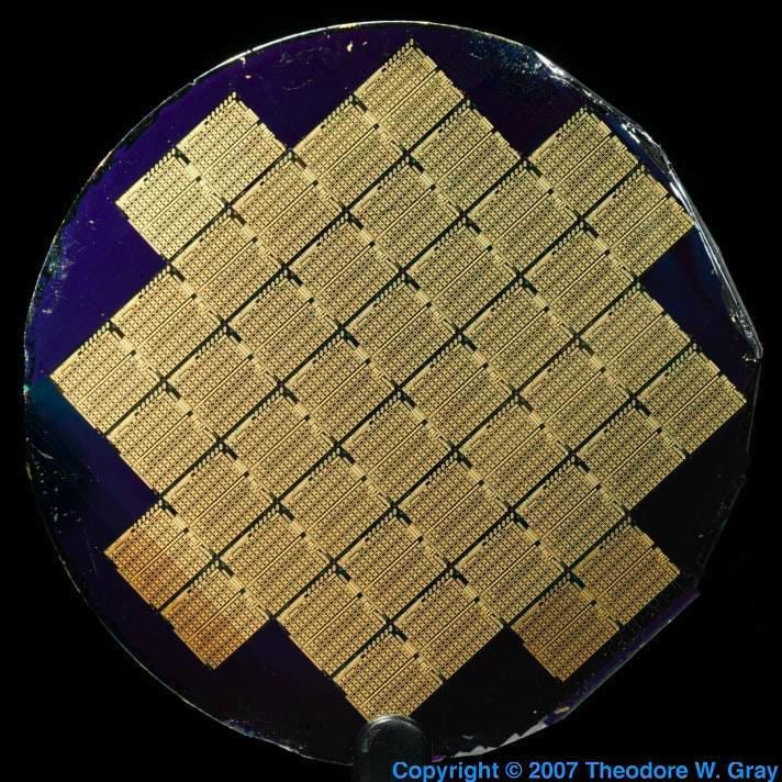
GaAs is often used as a substrate material for the epitaxial growth of other III-V semiconductors including indium gallium arsenide, aluminum gallium arsenide and others.
Preparation and chemistry
In the compound, gallium has a +3 oxidation state. Gallium arsenide single crystals can be prepared by three industrial processes:
Alternative methods for producing films of GaAs include:
3 → 2 GaAs + 3 Cl
2
3)
3 + AsH
3 → GaAs + 3 CH
4
4 → 4 GaAs or 2 Ga + As
2 → 2 GaAs
Oxidation of GaAs occurs in air and degrades performance of the semiconductor. The surface can be passivated by depositing a cubic gallium(II) sulfide layer using a tert-butyl gallium sulfide compound such as (t
BuGaS)
7.
Semi-insulating crystals
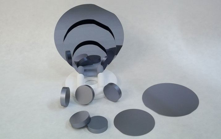
If a GaAs boule is grown with excess arsenic present, it gets certain defects, in particular arsenic antisite defects (an arsenic atom at a gallium atom site within the crystal lattice). The electronic properties of these defects (interacting with others) cause the Fermi level to be pinned to near the center of the bandgap, so that this GaAs crystal has very low concentration of electrons and holes. This low carrier concentration is similar to an intrinsic (perfectly undoped) crystal, but much easier to achieve in practice. These crystals are called "semi-insulating", reflecting their high resistivity of 107–109 Ω·cm (which is quite high for a semiconductor, but still much lower than a true insulator like glass).
Etching
Wet etching of GaAs industrially uses an oxidizing agent such as hydrogen peroxide or bromine water, and the same strategy has been described in a patent relating to processing scrap components containing GaAs where the Ga3+
is complexed with a hydroxamic acid ("HA"), for example:
2O
2 + "HA" → "GaA" complex + H
3AsO
4 + 4 H
2O
This reaction produces arsenic acid.
GaAs digital logic
GaAs can be used for various transistor types:
The HBT can be used in integrated injection logic (I2L). The earliest GaAs logic gate used Buffered FET Logic (BFL).
From ~1975 to 1995 the main logic families used were:
GaAs advantages
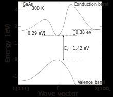
Some electronic properties of gallium arsenide are superior to those of silicon. It has a higher saturated electron velocity and higher electron mobility, allowing gallium arsenide transistors to function at frequencies in excess of 250 GHz. GaAs devices are relatively insensitive to overheating owing to their wider energy bandgap, and they also tend to create less noise in electronic circuits than silicon devices, especially at high frequencies. This is a result of higher carrier mobilities and lower resistive device parasitics. These superior properties are compelling reasons to use GaAs circuitry in mobile phones, satellite communications, microwave point-to-point links and higher frequency radar systems. It is also used in the manufacture of Gunn diodes for the generation of microwaves.
Another advantage of GaAs is that it has a direct band gap, which means that it can be used to absorb and emit light efficiently. Silicon has an indirect bandgap and so is relatively poor at emitting light.
As a wide direct band gap material with resulting resistance to radiation damage, GaAs is an excellent material for outer space electronics and optical windows in high power applications.
Because of its wide bandgap, pure GaAs is highly resistive. Combined with a high dielectric constant, this property makes GaAs a very good substrate for Integrated circuits and unlike Si provides natural isolation between devices and circuits. This has made it an ideal material for monolithic microwave integrated circuits, MMICs, where active and essential passive components can readily be produced on a single slice of GaAs.
One of the first GaAs microprocessors was developed in the early 1980s by the RCA corporation and was considered for the Star Wars program of the United States Department of Defense. These processors were several times faster and several orders of magnitude more radiation proof than silicon counterparts, but were more expensive. Other GaAs processors were implemented by the supercomputer vendors Cray Computer Corporation, Convex, and Alliant in an attempt to stay ahead of the ever-improving CMOS microprocessor. Cray eventually built one GaAs-based machine in the early 1990s, the Cray-3, but the effort was not adequately capitalized, and the company filed for bankruptcy in 1995.
Complex layered structures of gallium arsenide in combination with aluminium arsenide (AlAs) or the alloy AlxGa1−xAs can be grown using molecular beam epitaxy (MBE) or using metalorganic vapor phase epitaxy (MOVPE). Because GaAs and AlAs have almost the same lattice constant, the layers have very little induced strain, which allows them to be grown almost arbitrarily thick. This allows extremely high performance and high electron mobility HEMT transistors and other quantum well devices.
Concerns over GaAs's susceptibility to heat damage have been raised, but it has been speculated that certain manufacturers would benefit from such limitations, considering the planned obsolescence cycle that many consumer electronics are designed to follow.
Silicon advantages
Silicon has three major advantages over GaAs for integrated circuit manufacture. First, silicon is abundant and cheap to process in the form of silicate minerals. The economies of scale available to the silicon industry has also hindered the adoption of GaAs.
In addition, a Si crystal has a very stable structure and can be grown to very large diameter boules and processed with very good yields. It is also a fairly good thermal conductor, thus enabling very dense packing of transistors that need to get rid of their heat of operation, all very desirable for design and manufacturing of very large ICs. Such good mechanical characteristics also makes it a suitable material for the rapidly developing field of nanoelectronics. Naturally, GaAs surface cannot withstand the high temperature needed for diffusion; however a viable and actively pursued alternative as of the 1980s was ion implanation.
The second major advantage of Si is the existence of a native oxide (silicon dioxide, SiO2), which is used as an insulator in electronic devices. Silicon dioxide can easily be incorporated onto silicon circuits, and such layers are adherent to the underlying silicon. SiO2 is not only a good insulator (with a band gap of 8.9 eV), but the Si-SiO2 interface can be easily engineered to have excellent electrical properties, most importantly low density of interface states. GaAs does not have a native oxide, not easily support a stable adherent insulating layer, and not possess the dielectric strength or surface passivating qualities of the Si-SiO2.
Aluminum oxide (Al2O3) has been extensively studied as a possible gate oxide for GaAs (as well as InGaAs).
The third advantage of silicon is that it possesses a higher hole mobility compared to GaAs (500 versus 400 cm2V−1s−1). This high mobility allows the fabrication of higher-speed P-channel field effect transistors, which are required for CMOS logic. Because they lack a fast CMOS structure, GaAs circuits must use logic styles which have much higher power consumption; this has made GaAs logic circuits unable to compete with silicon logic circuits.
For manufacturing solar cells, silicon has relatively low absorptivity for the sunlight meaning about 100 micrometers of Si is needed to absorb most sunlight. Such a layer is relatively robust and easy to handle. In contrast, the absorptivity of GaAs is so high that only a few micrometers of thickness are needed to absorb all of the light. Consequently, GaAs thin films must be supported on a substrate material.
Silicon is a pure element, avoiding the problems of stoichiometric imbalance and thermal unmixing of GaAs.
Silicon has a nearly perfect lattice, impurity density is very low and allows very small structures to be built (currently down to 16 nm). GaAs in contrast has a very high impurity density, which makes it difficult to build integrated circuits with small structures, so the 500 nm process is a common process for GaAs.
Solar cells and detectors
Gallium arsenide (GaAs) is an important semiconductor material for high-cost, high-efficiency solar cells and is used for single-crystalline thin film solar cells and for multi-junction solar cells.
In 1970, the first GaAs heterostructure solar cells were created by the team led by Zhores Alferov in the USSR. In the early 1980s, the efficiency of the best GaAs solar cells surpassed that of conventional, crystalline silicon-based solar cells. In the 1990s GaAs solar cells took over from silicon as the cell type most commonly used for photovoltaic arrays for satellite applications. Later, dual- and triple-junction solar cells based on GaAs with germanium and indium gallium phosphide layers were developed as the basis of a triple-junction solar cell, which held a record efficiency of over 32% and can operate also with light as concentrated as 2,000 suns. This kind of solar cell powers the rovers Spirit and Opportunity, which are exploring Mars' surface. Also many solar cars utilize GaAs in solar arrays.
GaAs-based devices hold the world record for the highest-efficiency single-junction solar cell at 28.8%. This high efficiency is attributed to the extreme high quality GaAs epitaxial growth, surface passivation by the AlGaAs, and the promotion of photon recycling by the thin film design.
Complex designs of AlxGa1−xAs-GaAs devices can be sensitive to infrared radiation (QWIP).
GaAs diodes can be used for the detection of X-rays.
Light-emission devices
GaAs has been used to produce near-infrared laser diodes since 1962.
Fiber optic temperature measurement
For this purpose an optical fiber tip of an optical fiber temperature sensor is equipped with a gallium arsenide crystal. Starting at a light wavelength of 850 nm GaAs becomes optically translucent. Since the position of the band gap is temperature dependent, it shifts about 0.4 nm/K. The measurement device contains a light source and a device for the spectral detection of the band gap. With the changing of the band gap (0.4 nm/K) an algorithm calculates the temperature (all 250 ms).
Spin-charge converters
GaAs may have applications in spintronics as it can be used instead of platinum in spin-charge converters and may be more tunable.
Safety
The environment, health and safety aspects of gallium arsenide sources (such as trimethylgallium and arsine) and industrial hygiene monitoring studies of metalorganic precursors have been reported. California lists gallium arsenide as a carcinogen, as do IARC and ECA, and it is considered a known carcinogen in animals. However, a 2013 review (funded by industry) argued against these classifications, saying that when rats or mice inhale fine GaAs powders (as in previous studies), they get cancer from the resulting lung irritation and inflammation, rather than from a primary carcinogenic effect of the GaAs itself—and that moreover fine GaAs powders are unlikely to be created in the production or use of GaAs.