
 | ||
Produced From March 1976 to present Common manufacturer(s) Mostek, Synertek, Zilog, SGS-Thomson, NEC, Sharp, Toshiba, Rohm, GoldStar, Hitachi, National Semiconductor, and others. Max. CPU clock rate 2.5 MHz to 8 MHz with CMOS variant up to 20 MHz | ||
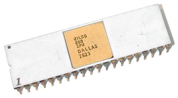
The Z80 CPU is an 8-bit based microprocessor. It was introduced by Zilog in 1976 as the startup company's first product. The Z80 was conceived by Federico Faggin in late 1974 and developed by him and his then-11 employees at Zilog from early 1975 until March 1976, when the first fully working samples were delivered. With the revenue from the Z80, the company built its own chip factories and grew to over a thousand employees over the following two years.
Contents
- History
- Programming model and register set
- Registers
- Datapoint 2200 and Intel 8008
- New syntax
- Instruction set and encoding
- Undocumented instructions
- Bugs
- Example code
- Instruction execution
- Compatible peripherals
- Desktop computers
- Embedded systems and consumer electronics
- Industry
- Consumer electronics
- Musical instruments
- References
The Zilog Z80 was a software compatible extension and enhancement of the Intel 8080 and, like it, was mainly aimed at embedded systems. According to the designers, the primary targets for the Z80 CPU (and its optional support and peripheral ICs) were products like intelligent terminals, high end printers and advanced cash registers as well as telecom equipment, industrial robots and other kinds of automation equipment.
The Z80 was officially introduced on the market in July 1976 and came to be widely used also in general desktop computers using CP/M and other operating systems as well as in the home computers of the 1980s. It was also common in military applications, musical equipment, such as synthesizers, and in the computerized coin operated video games of the late 1970s and early 1980, the arcade machines or video game arcade cabinets.
In the early 1980s, the Z80 was the most commonly used CPU of all time, and, along with the MOS Technology 6502 family, dominated the home computer market from the late 1970s to the mid 1980s.
Zilog licensed the Z80 to the US-based Synertek and Mostek, that had helped them with initial production, as well as to a European second source manufacturer, SGS. The design was copied also by several Japanese, East European and Russian manufacturers. This enabled the Z80 to gain acceptance in the world market since large companies like NEC, Toshiba, Sharp, and Hitachi, started to manufacture the device (or their own Z80 compatible designs). In recent decades Zilog has refocused on the ever-growing market for embedded systems (for which the original Z80 and the Z180 were designed) and the most recent Z80-compatible microcontroller family, the fully pipelined 24-bit eZ80 with a linear 16 MB address range, has been successfully introduced alongside the simpler Z180 and Z80 products.
History
The Z80 came about when physicist Federico Faggin left Intel at the end of 1974 to found Zilog with Ralph Ungermann. At Fairchild Semiconductor, and later at Intel, Faggin had been working on fundamental transistor and semiconductor manufacturing technology. He also developed the basic design methodology used for memories and microprocessors at Intel and led the work on the Intel 4004, the 8080 and several other ICs. Masatoshi Shima, the principal logic and transistor level-designer of the 4004 and the 8080 under Faggin's supervision, also joined the Zilog team.
By March 1976, Zilog had developed the Z80 as well as an accompanying assembler based development system for its customers, and by July 1976, this was formally launched onto the market. (Some of the Z80 support and peripheral ICs were under development at this point, and many of them were launched during the following year.)
Early Z80s were manufactured by Synertek and Mostek, before Zilog had its own manufacturing factory ready, in late 1976. These companies were chosen because they could do the ion implantation needed to create the depletion-mode MOSFETs that the Z80 design used as load transistors in order to cope with a single 5 Volt power supply.
Faggin designed the instruction set to be binary compatible with the Intel 8080 so that most 8080 code, notably the CP/M operating system and Intel's PL/M compiler for 8080 (as well as its generated code), would run unmodified on the new Z80 CPU. Masatoshi Shima designed most of the microarchitecture as well as the gate and transistor levels of the Z80 CPU, assisted by a small number of engineers and layout people. CEO Federico Faggin was actually heavily involved in the chip layout work, together with two dedicated layout people. Faggin worked 80 hours a week in order to meet the tight schedule given by the financial investors, according to himself.
The Z80 offered many improvements over the 8080:
The Z80 took over from the 8080 and its offspring, the 8085, in the processor market, and became one of the most popular 8-bit CPUs. Perhaps a key to the initial success of the Z80 was the built-in DRAM refresh, and other features which allowed systems to be built with fewer support chips (Z80 embedded systems typically use static RAM and hence do not need this refresh).
For the original NMOS design, the specified upper clock frequency limit increased successively from the introductory 2.5 MHz, via the well known 4 MHz (Z80A), up to 6 (Z80B) and 8 MHz (Z80H). CMOS versions were also developed with specified upper frequency limits ranging from 4 MHz up to 20 MHz for the version sold today. The CMOS versions also allowed low-power sleep with internal state retained, having no lower frequency limit. The fully compatible derivatives HD64180/Z180 and eZ80 are currently specified for up to 33 and 50 MHz respectively.
Programming model and register set
The programming model and register set are fairly conventional, ultimately based on the register structure of the Datapoint 2200 (which the related 8086 family also inherited). The Z80 was designed as an extension of the 8080, created by the same engineers, which in turn was an extension of the 8008 and the Datapoint 2200. These early designs allowed register H and L to be paired into a 16-bit address register HL. In the 8080 this pairing was generalized into BC and DE, while HL also became usable as a 16-bit accumulator. The Z80 orthogonalized this a bit further by making all 16-bit register pairs (including IX and IY) more general purpose, with 16-bit copying directly to and from memory. The new 16-bit IX and IY registers are primarily intended as base address-registers, where a particular instruction supplies a constant offset, but they are also usable as 16-bit accumulators, among other things. The Z80 also introduces a new signed overflow flag and complements the fairly simple 16-bit arithmetics of the 8080 with dedicated instructions for signed 16-bit arithmetics.
The 8080 compatible registers AF, BC, DE, HL are duplicated as two separate banks in the Z80, where the processor can quickly switch from one bank to the other; a feature useful for speeding up responses to single-level, high-priority interrupts. A similar feature was present in the Datapoint 2200 but was never implemented at Intel. The dual register-set makes sense as the Z80 (like most microprocessors at the time) was really intended for embedded use, not for personal computers, or the yet-to-be invented home computers. According to one of the designers, Masatoshi Shima, the market focus was on high performance printers, high-end cash registers, and intelligent terminals, although Ralph Ungermann also saw other opportunities, such as computers. The two register sets also turned out to be quite useful for heavily optimized manual assembly-language coding, such as for floating point arithmetics or home computer games.
Registers
As on the 8080, 8-bit registers are typically paired to provide 16-bit versions. The 8080 compatible registers are:
AF: 8-bit accumulator (A) and flag bits (F) carry, zero, minus, parity/overflow, half-carry (used for BCD), and an Add/Subtract flag (usually called N) also for BCDBC: 16-bit data/address register or two 8-bit registersDE: 16-bit data/address register or two 8-bit registersHL: 16-bit accumulator/address register or two 8-bit registersSP: stack pointer, 16 bitsPC: program counter, 16 bitsThe new registers introduced with the Z80 are:
IX: 16-bit index or base register for 8-bit immediate offsetsIY: 16-bit index or base register for 8-bit immediate offsetsI: interrupt vector base register, 8 bitsR: DRAM refresh counter, 8 bits (msb does not count)AF': alternate (or shadow) accumulator and flags (toggled in and out with EX AF,AF' )BC', DE' and HL': alternate (or shadow) registers (toggled in and out with EXX)There is no direct access to the alternate registers; instead, two special instructions, EX AF,AF' and EXX, each toggles one of two multiplexer flip-flops. This enables fast context switches for interrupt service routines: EX AF, AF' may be used alone, for really simple and fast interrupt routines, or together with EXX to swap the whole BC, DE, HL set. This is still several times as fast as pushing the same registers on the stack. Slower, lower priority, or multi level interrupts normally use the stack to store registers, however.
The refresh register, R, increments each time the CPU fetches an opcode (or opcode prefix) and has therefore no simple relationship with program execution. This has sometimes been used to generate pseudorandom numbers in games, and also in software protection schemes. It has also been employed as a "hardware" counter in some designs; an example of this is the ZX81, which lets it keep track of character positions on the TV screen by triggering an interrupt at wrap around (by connecting INT to A6).
The interrupt vector register, I, is used for the Z80 specific mode 2 interrupts (selected by the IM 2 instruction). It supplies the high byte of the base address for a 128-entry table of service routine addresses which are selected via an index sent to the CPU during an interrupt acknowledge cycle; this index is simply the low byte part of the pointer to the tabulated indirect address pointing to the service routine. The pointer identifies a particular peripheral chip and/or peripheral function or event, where the chips are normally connected in a so-called daisy chain for priority resolution. Like the refresh register, this register has also sometimes been used creatively; in interrupt modes 0 and 1 (or in a system not using interrupts) it can be used as simply another 8-bit data register.
The instructions LD A,R and LD A,I affect the Z80 flags register, unlike all the other LD (load) instructions. The Sign (bit 7) and Zero (bit 6) flags are set according to the data loaded from the Refresh or Interrupt source registers. For both instructions, the Parity/Overflow flag (bit 2) is set according to the current state of the IFF2 flip-flop.
Datapoint 2200 and Intel 8008
The first Intel 8008 assembly language was based on a very simple (but systematic) syntax inherited from the Datapoint 2200 design. This original syntax was later transformed into a new, somewhat more traditional, assembly language form for this same original 8008 chip. At about the same time, the new assembly language was also extended to accommodate the added addressing possibilities in the more advanced Intel 8080 chip (the 8008 and 8080 shared a language subset without being binary compatible; however, the 8008 was binary compatible with the Datapoint 2200).
In this process, the mnemonic L, for LOAD, was replaced by various abbreviations of the words LOAD, STORE and MOVE, intermixed with other symbolic letters. The mnemonic letter M, for memory (referenced by HL), was lifted out from within the instruction mnemonic to become a syntactically freestanding operand, while registers and combinations of registers became very inconsistently denoted; either by abbreviated operands (MVI D, LXI H and so on), within the instruction mnemonic itself (LDA, LHLD and so on), or both at the same time (LDAX B, STAX D and so on).
Illustration of four syntaxes, using samples of equivalent, or (for 8086) very similar, load and store instructions. The Z80 syntax uses parentheses around an expression to indicate that the value should be used as a memory address (as mentioned below), while the 8086 syntax uses brackets instead of ordinary parentheses for this purpose. Both Z80 and 8086 use the + sign to indicate that a constant is added to a base register to form an address
New syntax
Because Intel had a copyright on their assembly mnemonics, a new assembly syntax had to be developed for the Z80. This time a more systematic approach was used:
These principles made it straightforward to find names and forms for all new Z80 instructions, as well as orthogonalizations of old ones, such as LD BC,(1234).
Apart from naming differences, and despite a certain discrepancy in basic register structure, the Z80 and 8086 syntax are virtually isomorphic for a large portion of instructions. Only quite superficial similarities (such as the word MOV, or the letter X, for extended register) exist between the 8080 and 8086 assembly languages, although 8080 programs can be assembled into 8086 object code using a special assembler or translated to 8086 assembly language by a translator program.
Instruction set and encoding
The Z80 uses 252 out of the available 256 codes as single byte opcodes ("root instruction"); the four remaining codes are used extensively as opcode prefixes: CB and ED enable extra instructions and DD or FD selects IX+d or IY+d respectively (in some cases without displacement d) in place of HL. This scheme gives the Z80 a large number of permutations of instructions and registers; Zilog categorizes these into 158 different "instruction types", 78 of which are the same as those of the Intel 8080 (allowing operation of most 8080 programs on a Z80). The Zilog documentation further groups instructions into the following categories:
No multiply instruction is available in the original Z80. Different sizes and variants of additions, shifts, and rotates have somewhat differing effects on flags because most of the flag-changing properties of the 8080 were copied.
The Z80 has four new LD instructions that can load the DE and BC register pairs from memory, and load memory from these two register pairs -- unlike the 8080. As on the 8080, load instructions do not affect the flags (except for the special purpose I and R register loads). A quirk (common with the 8080) of the register-to-register load instructions is that each of the 8-bit registers can be loaded from themselves (e.g. LD A,A). This is effectively a NOP.
Unlike the 8080, the Z80 can jump to a relative address using a signed 8-bit displacement. Only the Zero and Carry flags can be tested for these new two-byte JR instructions.
A two-byte instruction specialized for program looping is new to the Z80. DJNZ (Decrement Jump if Non-Zero) takes a signed 8-bit displacement as an immediate operand. The B register is decremented. If the result is nonzero then program execution jumps relative to the address of the PC plus the displacement. The flags remain unaltered. To perform an equivalent loop on an 8080 would require separate decrement and jump (to a two-byte absolute address) instructions, and the flag register would be altered.
The index register (IX/IY) instructions can be useful for accessing data organised in fixed heterogenous structures (such as records) or at fixed offsets relative a variable base address (as in recursive stack frames) and can also reduce code size by removing the need for multiple short instructions using non-indexed registers. However, although they may save speed in some contexts when compared to long/complex "equivalent" sequences of simpler operations, they incur a lot of additional CPU time (e.g. 19 T-states to access one indexed memory location vs. as little as 11 to access the same memory using HL and INCrement it to point to the next). Thus, for simple or linear accesses of data, IX and IY tend to be slower. Still, they may be useful in cases where the 'main' registers are all occupied, by removing the need to save/restore registers. Their officially undocumented 8-bit halves (see below) can be especially useful in this context, for they incur less slowdown than their 16-bit parents. Similarly, instructions for 16-bit additions are not particularly fast (11 clocks) in the original Z80; nonetheless, they are about twice as fast as performing the same calculations using 8-bit operations, and equally important, they reduce register usage.
The 10-year-newer microcoded Z180 design could initially afford more "chip area", permitting a slightly more efficient implementation (using a wider ALU, among other things); similar things can be said for the Z800, Z280, and Z380. However, it was not until the fully pipelined eZ80 was launched in 2001 that those instructions finally became approximately as cycle-efficient as it is technically possible to make them, i.e. given the Z80 encodings combined with the capability to do an 8-bit read or write every clock cycle.
Undocumented instructions
The index registers, IX and IY, were intended as flexible 16 bit pointers, enhancing the ability to manipulate memory, stack frames and data structures. Officially, they were treated as 16-bit only. In reality, they were implemented as a pair of 8-bit registers, in the same fashion as the HL register, which is accessible either as 16 bits or separately as the High and Low registers. Even the binary opcodes (machine language) were identical, but preceded by a new opcode prefix. Zilog published the opcodes and related mnemonics for the intended functions, but did not document the fact that every opcode that allowed manipulation of the H and L registers was equally valid for the 8 bit portions of the IX and IY registers. As an example, the opcode 26h followed by an immediate byte value (LD H,n) will load that value into the H register. Preceding this two-byte instruction with the IX register's opcode prefix, DD, would instead result in the most significant 8 bits of the IX register being loaded with that same value. A notable exception to this would be instructions similar to LD H,(IX+d) which make use of both the HL and IX or IY registers in the same instruction; in this case the DD prefix is only applied to the (IX+d) portion of the instruction.
There are several other undocumented instructions as well. Undocumented or illegal opcodes are not detected by the Z80 and have various effects, some of which are useful. However, as they are not part of the formal definition of the instruction set, different implementations of the Z80 are not guaranteed to work the same way for every undocumented opcode.
Bugs
The OTDR instruction doesn't conform to the Z80 documentation. Both OTDR and OTIR are supposed to leave the carry C unaffected. OTIR functions correctly; however, during the execution of the OTDR instruction, the carry takes the results of a spurious compare between the accumulator and what has last been output by the OTDR instruction.
Example code
The following Z80 assembly source code is for a subroutine named memcpy that copies a block of data bytes of a given size from one location to another. Important: The example code does not handle a certain case where the destination block overlaps the source; a fatal bug. The sample code is extremely inefficient, intended to illustrate various instruction types, rather than best practices for speed. In particular, the Z80 has a single instruction that will execute the entire loop (LDIR). The data block is copied one byte at a time, and the data movement and looping logic utilizes 16-bit operations. Note that the assembled code is binary-compatible with the Intel 8080 and 8085 CPUs.
Instruction execution
Each instruction is executed in steps that are usually termed machine cycles (M-cycles), each of which can take between three and six clock periods (T-cycles). Each M-cycle corresponds roughly to one memory access and/or internal operation. Many instructions actually end during the M1 of the next instruction which is known as a fetch/execute overlap.
The Z80 machine cycles are sequenced by an internal state machine which builds each M-cycle out of 3, 4, 5 or 6 T-cycles depending on context. This avoids cumbersome asynchronous logic and makes the control signals behave consistently at a wide range of clock frequencies. It also means that a higher frequency crystal must be used than without this subdivision of machine cycles (approximately 2–3 times higher). It does not imply tighter requirements on memory access times, however, as a high resolution clock allows more precise control of memory timings and memory therefore can be active in parallel with the CPU to a greater extent (i.e. sitting less idle), allowing more efficient use of available memory bandwidth.
One central example of this is that, for opcode fetch, the Z80 combines two full clock cycles into a memory access period (the M1-signal). In the Z80 this signal therefore lasts for a much larger (relative) part of the typical instruction execution time than in a more asynchronous processor design such as the 6800, 6502, or similar, where this period would typically last only a (rather imprecise) fraction (typically 30-40%) of a clock cycle. With memory chip affordability (i.e. access times around 450-250 ns in the 1980s) typically determining the fastest possible access time, this meant that such designs were locked to a significantly longer clock cycle (i.e. lower internal clock speed) than the Z80.
Memory, especially EPROM, but also Flash, were generally slow as compared to the state machine sub-cycles (clock cycles) used in contemporary microprocessors. The shortest machine cycle that could safely be used in embedded designs has therefore often been limited by memory access times, not by the maximum CPU frequency (especially so during the home computer era). However, this relation has slowly changed during the last decades, particularly regarding SRAM; cacheless, single-cycle designs such as the eZ80 have therefore become much more meaningful recently.
The content of the refresh register R is sent out on the lower half of the address bus along with a refresh control signal while the CPU is decoding and executing the fetched instruction. During refresh the contents of the Interrupt register I are sent out on the upper half of the address bus.
Compatible peripherals
Zilog introduced a number of peripheral parts for the Z80, which all supported the Z80's interrupt handling system and I/O address space. These included the Counter/Timer Channel (CTC), the SIO (Serial Input Output), the DMA (Direct Memory Access), the PIO (Parallel Input-Output) and the DART (Dual Asynchronous Receiver Transmitter). As the product line developed, low-power, high-speed and CMOS versions of these chips were produced.
Like the 8080, 8085 and 8086 processors, but unlike processors such as the Motorola 6800 and MOS Technology 6502, the Z80 and 8080 had a separate control line and address space for I/O instructions. While some Z80-based computers such as the Osborne 1 used "Motorola-style" memory mapped input/output devices, usually the I/O space was used to address one of the many Zilog peripheral chips compatible with the Z80. Zilog I/O chips supported the Z80's new mode 2 interrupts which simplified interrupt handling for large numbers of peripherals.
The Z80 was officially described as supporting 16-bit (64 KB) memory addressing, and 8-bit (256 ports) I/O-addressing. All I/O instructions actually assert the entire 16-bit address bus. OUT (C),reg and IN reg,(C) places the contents of the entire 16 bit BC register on the address bus; OUT (n),A and IN A,(n) places the contents of the A register on b8-b15 of the address bus and n on b0-b7 of the address bus. A designer could choose to decode the entire 16 bit address bus on I/O operations in order to take advantage of this feature, or use the high half of the address bus to select subfeatures of the I/O device. This feature has also been used to minimise decoding hardware requirements, such as in the Amstrad CPC/PCW and ZX81.
Desktop computers
During the late 1970s and early 1980s, the Z80 was used in a great number of fairly anonymous business-oriented machines with the CP/M operating system, a combination that dominated the market at the time. Two well-known examples of Z80+CP/M business computers are the portable Osborne 1 and the Kaypro series. Research Machines manufactured the 380Z and 480Z microcomputers which were networked with a thin Ethernet type LAN and CP/NET in 1981. Other manufacturers of such systems included Televideo, Xerox (820 range) and a number of more obscure firms. Some systems used multi-tasking operating system software to share the one processor between several concurrent users.
In the U.S., the Radio Shack TRS-80, introduced in 1977, as well as the Models II, III, 4, and the proposed Model V, used the Z80. In the United Kingdom, Sinclair Research used the Z80 and Z80A in its ZX80, ZX81 and, ZX Spectrum home computers. Amstrad used them in their Amstrad CPC range and an early UK computer, the Nascom 1 and 2 also used the Z80. The Commodore 128 featured a Z80 processor alongside its MOS Technology 8502 processor for CP/M compatibility. Other 6502 architecture computers on the market at the time, such as the BBC Micro, Apple II, and the 6510 based Commodore 64, could make use of the Z80 with an external unit, a plug-in card, or an expansion ROM cartridge. The Microsoft Z-80 SoftCard for the Apple II was a particularly successful add-on card and one of Microsoft's few hardware products of the era.
In 1981, Multitech (later to become Acer) introduced the Microprofessor I, a simple and inexpensive training system for the Z80 microprocessor. Currently, it is still manufactured and sold by Flite Electronics International Limited in Southampton, England.
Embedded systems and consumer electronics
The Zilog Z80 has long been a popular microprocessor in embedded systems and microcontroller cores, where it remains in widespread use today. The following list provides examples of such applications of the Z80, including uses in consumer electronics products.