
 | ||
Static random-access memory (static RAM or SRAM) is a type of semiconductor memory that uses bistable latching circuitry (flip-flop) to store each bit. SRAM exhibits data remanence, but it is still volatile in the conventional sense that data is eventually lost when the memory is not powered.
Contents
- Characteristics
- Clock rate and power
- Embedded use
- In computers
- Hobbyists
- Non volatile SRAM
- By transistor type
- By function
- By feature
- By flip flop type
- Design
- SRAM operation
- Bus behavior
- References
The term static differentiates SRAM from DRAM (dynamic random-access memory) which must be periodically refreshed. SRAM is faster and more expensive than DRAM; it is typically used for CPU cache while DRAM is used for a computer's main memory.
Characteristics
Advantages:
Disadvantages:
Clock rate and power
The power consumption of SRAM varies widely depending on how frequently it is accessed; in some instances, it can use as much power as dynamic RAM, when used at high frequencies, and some ICs can consume many watts at full bandwidth. On the other hand, static RAM used at a somewhat slower pace, such as in applications with moderately clocked microprocessors, draws very little power and can have a nearly negligible power consumption when sitting idle – in the region of a few micro-watts. Several techniques have been proposed to manage power consumption of SRAM-based memory structures.
STATIC RAM exists primarily as:
Embedded use
SRAM in its dual-ported form is sometimes used for realtime digital signal processing circuits.
In computers
SRAM is also used in personal computers, workstations, routers and peripheral equipment: CPU register files, internal CPU caches and external burst mode SRAM caches, hard disk buffers, router buffers, etc. LCD screens and printers also normally employ static RAM to hold the image displayed (or to be printed). Static RAM was used for the main memory of some early personal computers such as the ZX80, TRS-80 Model 100 and Commodore VIC-20.
Hobbyists
Hobbyists, specifically homebuilt processor enthusiasts, often prefer SRAM due to the ease of interfacing. It is much easier to work with than DRAM as there are no refresh cycles and the address and data buses are directly accessible rather than multiplexed. In addition to buses and power connections, SRAM usually requires only three controls: Chip Enable (CE), Write Enable (WE) and Output Enable (OE). In synchronous SRAM, Clock (CLK) is also included.
Non-volatile SRAM
Non-volatile SRAMs, or nvSRAMs, have standard SRAM functionality, but they save the data when the power supply is lost, ensuring preservation of critical information. nvSRAMs are used in a wide range of situations – networking, aerospace, and medical, among many others – where the preservation of data is critical and where batteries are impractical.
By transistor type
By function
In 1990s, asynchronous SRAM used to be employed for fast access time. Asynchronous SRAM was used as main memory for small cache-less embedded processors used in everything from industrial electronics and measurement systems to hard disks and networking equipment, among many other applications. Nowadays, synchronous SRAM (e.g. DDR SRAM) is rather employed similarly like Synchronous DRAM – DDR SDRAM memory is rather used than asynchronous DRAM (Dynamic random-access memory). Synchronous memory interface is much faster as access time can be significantly reduced by employing pipeline architecture. Furthermore, as DRAM is much cheaper than SRAM, SRAM is often replaced by DRAM, especially in the case when large volume of data is required. SRAM memory is however much faster for random (not block / burst) access. Therefore, SRAM memory is mainly used for CPU cache, small on-chip memory, FIFOs or other small buffers.
By feature
By flip-flop type
Design
A typical SRAM cell is made up of six MOSFETs. Each bit in an SRAM is stored on four transistors (M1, M2, M3, M4) that form two cross-coupled inverters. This storage cell has two stable states which are used to denote 0 and 1. Two additional access transistors serve to control the access to a storage cell during read and write operations. In addition to such six-transistor (6T) SRAM, other kinds of SRAM chips use 4, 8, 10 (4T, 8T, 10T SRAM), or more transistors per bit. Four-transistor SRAM is quite common in stand-alone SRAM devices (as opposed to SRAM used for CPU caches), implemented in special processes with an extra layer of polysilicon, allowing for very high-resistance pull-up resistors. The principal drawback of using 4T SRAM is increased static power due to the constant current flow through one of the pull-down transistors.
This is sometimes used to implement more than one (read and/or write) port, which may be useful in certain types of video memory and register files implemented with multi-ported SRAM circuitry.
Generally, the fewer transistors needed per cell, the smaller each cell can be. Since the cost of processing a silicon wafer is relatively fixed, using smaller cells and so packing more bits on one wafer reduces the cost per bit of memory.
Memory cells that use fewer than four transistors are possible – but, such 3T or 1T cells are DRAM, not SRAM (even the so-called 1T-SRAM).
Access to the cell is enabled by the word line (WL in figure) which controls the two access transistors M5 and M6 which, in turn, control whether the cell should be connected to the bit lines: BL and BL. They are used to transfer data for both read and write operations. Although it is not strictly necessary to have two bit lines, both the signal and its inverse are typically provided in order to improve noise margins.
During read accesses, the bit lines are actively driven high and low by the inverters in the SRAM cell. This improves SRAM bandwidth compared to DRAMs – in a DRAM, the bit line is connected to storage capacitors and charge sharing causes the bitline to swing upwards or downwards. The symmetric structure of SRAMs also allows for differential signaling, which makes small voltage swings more easily detectable. Another difference with DRAM that contributes to making SRAM faster is that commercial chips accept all address bits at a time. By comparison, commodity DRAMs have the address multiplexed in two halves, i.e. higher bits followed by lower bits, over the same package pins in order to keep their size and cost down.
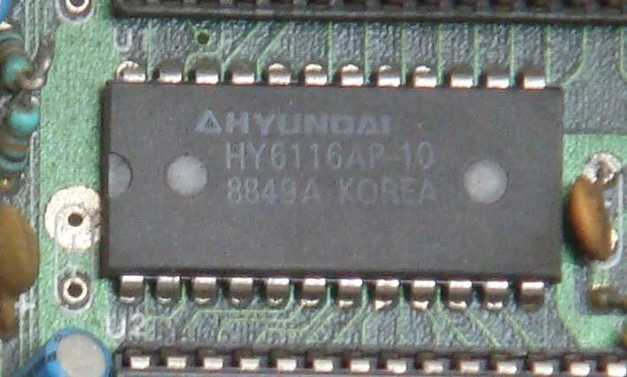
The size of an SRAM with m address lines and n data lines is 2m words, or 2m × n bits. The most common word size is 8 bits, meaning that a single byte can be read or written to each of 2m different words within the SRAM chip. Several common SRAM chips have 11 address lines (thus a capacity of 2m = 2,048 = 2k words) and an 8-bit word, so they are referred to as "2k × 8 SRAM".
SRAM operation
An SRAM cell has three different states: standby (the circuit is idle), reading (the data has been requested) or writing (updating the contents). SRAM operating in read mode and write modes should have "readability" and "write stability", respectively. The three different states work as follows:
Bus behavior
RAM with an access time of 70 ns will output valid data within 70 ns from the time that the address lines are valid. But the data will remain for a hold time as well (5–10 ns). Rise and fall times also influence valid timeslots with approximately 5 ns. By reading the lower part of an address range, bits in sequence (page cycle) one can read with significantly shorter access time (30 ns).