
Produced From late 1971 to 1981 Max. CPU clock rate 740 kHz Instruction set 4-bit BCD-oriented | Min. feature size 10 μm Transistors 2300 | |
 | ||
The Intel 4004 is a 4-bit central processing unit (CPU) released by Intel Corporation in 1971. It was the first commercially available microprocessor by Intel. The chip design started in April 1970, when Federico Faggin joined Intel, and it was completed under his leadership in January 1971. The first commercial sale of the fully operational 4004 occurred in March 1971 to Busicom Corp. of Japan for which it was originally designed and built as a custom chip. In mid-November of the same year, with the prophetic ad "Announcing a new era in integrated electronics", the 4004 was made commercially available to the general market. The 4004 is history’s first monolithic CPU, fully integrated in one small chip. Such a feat of integration was made possible by the use of the then-new silicon gate technology which allowed twice the number of random-logic transistors and an increase in speed by a factor of five compared to the incumbent technology. The 4004 microprocessor is one of 4 chips constituting the MCS-4 chip-set, which includes the 4001 ROM, 4002 RAM, and 4003 Shift Register. With these components, small computers with varying amounts of memory and I/O facilities can be built. Three other CPU chip designs were done at about the same time: the Four-Phase System AL1, done in 1969; the MP944, completed in 1970 and used in the F-14 Tomcat fighter jet; and the Texas Instruments TMS-0100 chip, announced in September 17, 1971. Both the AL1 and the MP944 use several chips for the implementation of the CPU function. The TMS0100 chip was presented as a “calculator on a chip” with the original designation TMS1802NC. This chip contains a very primitive CPU and can only be used to implement various simple 4-function calculators. It is the precursor of the TMS1000, introduced in 1974, which is considered the first microcontroller i.e., a computer on a chip containing not only the CPU, but also ROM, RAM, and I/O functions. The MCS-4 family of 4 chips developed by Intel, of which the 4004 is the CPU or microprocessor, is far more versatile and powerful than the single chip TMS1000, allowing the creation of a variety of small computers for various applications. The MCS-4 was eventually superseded by powerful microcontrollers like the Intel 8048 and the Zilog Z8 in 1978-1979. The architecture of this processor formed the basis for later models of microprocessors.
Contents
History and production
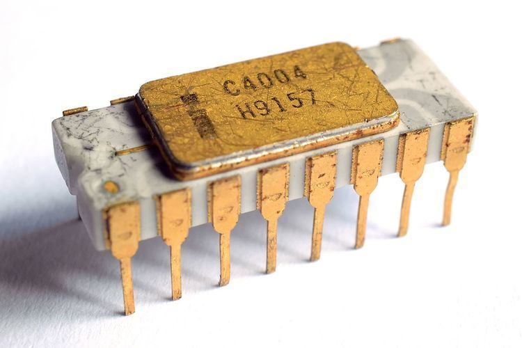
The first public mention of 4004 was an advertisement in the November 15, 1971 edition of Electronic News, though unconfirmed reports put the date of first delivery as early as March 1971. Packaged in a 16-pin ceramic dual in-line package, the 4004 was the first commercially available computer processor designed and manufactured by chip maker Intel, which had previously made semiconductor memory chips. The chief designers of the chip were Federico Faggin who created the design methodology and the silicon-based chip design, Ted Hoff who formulated the architecture, both of Intel, and Masatoshi Shima of Busicom who assisted in the development.
Faggin, the sole chip designer among the engineers on the MCS-4 project, was the only one with experience in metal-oxide semiconductor (MOS) random logic and circuit design. He also had the crucial knowledge of the new silicon gate process technology with self-aligned gates, which he had created at Fairchild in 1968. At Fairchild in 1968, Faggin also designed and manufactured the world's first commercial IC using SGT, the Fairchild 3708. As soon as he joined the Intel MOS Department he created a new random logic design methodology based on silicon gate, and contributed many technology and circuit design inventions that enabled their single chip microprocessor to become a reality. His methodology set the design style for all the early Intel microprocessors and later for the Zilog Z80. He also led the MCS-4 project and was responsible for its successful outcome (1970–1971). Marcian "Ted" Hoff, head of the Application Research Department, contributed the architectural proposal for Busicom working with Stanley Mazor in 1969, then he moved on to other projects. When asked where he got the ideas for the architecture of the first microprocessor, Hoff related that Plessey, "a British tractor company", had donated a minicomputer to Stanford, and he had "played with it some" while he was there. Shima designed the Busicom calculator firmware and assisted Faggin during the first six months of the implementation. The manager of Intel's MOS Design Department was Leslie L. Vadász. At the time of the MCS-4 development, Vadasz's attention was completely focused on the mainstream business of semiconductor memories and he left the leadership and the management of the MCS-4 project to Faggin.
Busicom had designed their own special-purpose LSI chipset for use in their Busicom 141-PF calculator with integrated printer, following the architectural model of the Olivetti Programma 101, the world’s first tabletop programmable calculator, introduced in 1965, and commissioned Intel to develop it for production. However, Intel determined it was too complex, since serial memories required more components, and would use 40 pins, a packaging standard different from Intel’s own 16-pin standard and so it was proposed that a new design produced with standard 16-pin DIP packaging and reduced instruction set be developed., using Intel’s newly developed dynamic RAM memory. This resulted in the 4004 architecture, which is part of a family of chips, including ROM, DRAM, and serial-to-parallel shift register chips. The 4004 was subsequently designed using silicon gate technology and built of approximately 2,300 transistors and was followed the next year by the first ever 8-bit microprocessor, the 3,500 transistor 8008 (and the 4040, a revised and improved 4004). It was not until the development of the 40-pin 8080 in 1974 that the address and data buses would be separated, giving faster and simpler access to memory.
The 4004 employs a 10 µm process silicon-gate enhancement load pMOS technology on a 12 mm² die and can execute approximately 92,000 instructions per second; a single instruction cycle is 10.8 microseconds. The original clock rate design goal was 1 MHz, the same as the IBM 1620 Model I.
The Intel 4004 was designed by physically cutting sheets of Rubylith into thin strips to lay out the circuits to be printed, a process made obsolete by current computer graphic design capabilities.
For the purpose of testing the produced chips, Faggin developed a tester for silicon waffers of MCS-4 family that was itself driven by 4004 chip. The tester also served as a proof for the management that Intel 4004 microprocessor could be used not only in calculator-like products, but also for control applications.
Name and variants
When Faggin designed the MCS-4 family, he also christened the chips with distinct names: 4001, 4002, 4003, and 4004, breaking away from the numbering scheme used by Intel at that time which would have required the names 1302, 1105, 1507, and 1202 respectively. Had he followed Intel's number sequence, the idea that the chips were part of a family of components intended to work seamlessly together would have been lost. Intel's early numbering scheme for integrated circuits used a four-digit number for each component. The first digit indicated the process technology used, the second digit indicated the generic function, and the last two digits of the number were used to indicate the sequential number in the development of the component. The 8008 microprocessor was originally called 1201, per Intel’s naming conventions. Before its market introduction, the 1201 was renamed 8008, following the new naming convention started with the 4001/2/3/4.
Tadashi Sasaki attributes the basic invention to break the calculator into four parts with ROM (4001), RAM (4002), shift registers (4003) and CPU (4004) to an unnamed woman from the Nara Women's College present at a brainstorming meeting that was held in Japan prior to his first meeting with Robert Noyce from Intel, leading up to the Busicom deal.
The 4004 is part of the MCS-4 family of LSI chips that can be used to build digital computers with varying amounts of memory. The other members of the MCS-4 family are memories and input/output circuits, which are necessary to implement a complete computer. The 4001 is a ROM (read-only memory) with four lines of output; the 4002 is a RAM (random access memory) with four lines of input/output. The 4003 is a static shift register to be used for expanding the I/O lines; e.g., for keyboard scanning or controlling a printer.
The 4004 includes control functions for memory and I/O, which are not normally handled by the microprocessor.
Technical specifications
Support chips
The minimum system specification described by Intel consists of a 4004 with a single 256-byte 4001 program ROM; there is no explicit need for separate RAM in minimal complexity applications thanks to the 4004's large number of onboard index registers, which represent the equivalent of 16 x 4-bit or 8 x 8-bit characters (or a mixture) of working RAM, nor for simple interface chips thanks to its built-in I/O lines. However, as project complexity increases, the various other support chips start to become useful.
Packaging
Numerous versions of the Intel MCS-4 line of processors were produced. The earliest versions, marked C (like C4004), were ceramic and used a zebra pattern of white and gray on the back of the chips, often called "grey traces". The next generation of the chips was plain white ceramic (also marked C), and then dark grey ceramic (D). Many of the more recent versions of MCS-4 family were also produced with plastic (P).
Use
The first commercial product to use a microprocessor was the Busicom calculator 141-PF. The 4004 was also used in the first microprocessor-controlled pinball game, a prototype produced by Dave Nutting Associates for Bally in 1974.
According to Nick Tredennick, a microprocessor designer and expert witness to the Boone/Hyatt patent case:
Here are my opinions from [the] study [I conducted for the patent case]. The first microprocessor in a commercial product was the Four Phase Systems AL1. The first commercially available (sold as a component) microprocessor was the 4004 from Intel.
A popular myth has it that Pioneer 10, the first spacecraft to leave the solar system, used an Intel 4004 microprocessor. According to Dr. Larry Lasher of Ames Research Center, the Pioneer team did evaluate the 4004, but decided it was too new at the time to include in any of the Pioneer projects. The myth was repeated by Federico Faggin himself in a lecture for the Computer History Museum in 2006.
Legacy and value
Faggin put his sign on the microprocessor; in a corner of the die you can read "F.F."
On November 15, 2006, the 35th anniversary of the 4004, Intel celebrated by releasing the chip's schematics, mask works, and user manual. A fully functional 41 x 58 cm, 130x scale replica of the Intel 4004 was built using discrete transistors and put on display in 2006 at the Intel Museum in Santa Clara, California.
On October 15, 2010, Faggin, Hoff, and Mazor were awarded the National Medal of Technology and Innovation by President Barack Obama for their pioneering work on the 4004.