
Max. CPU clock rate 1 MHz to 2 MHz Transistors 3,510 | Instruction set MOS 6502 Instructions 56 | |
 | ||
Produced 1975; 42 years ago (1975) Common manufacturer(s) | ||
The MOS Technology 6502 (typically "sixty-five-oh-two" or "six-five-oh-two") is an 8-bit microprocessor that was designed by a small team led by Chuck Peddle for MOS Technology. When it was introduced in 1975, the 6502 was, by a considerable margin, the least expensive full-featured microprocessor on the market. It initially sold for less than one-sixth the cost of competing designs from larger companies, such as Motorola and Intel, and caused rapid decreases in pricing across the entire processor market. Along with the Zilog Z80 it sparked a series of projects that resulted in the home computer revolution of the early 1980s.
Contents
- Origins at Motorola
- Moving to MOS Technology
- Introducing the 6501 and 6502
- Motorola lawsuit
- Computers and games
- Technical description
- Registers
- Addressing
- Indirect addressing
- Detailed behavior
- Assembly language instructions
- Variations and derivatives
- 6512
- 16 bit derivatives
- 32 bit derivatives
- Example code
- Bugs and quirks
- Acceleration
- Works cited
- References
Popular home video game consoles and computers, such as Atari, Apple II, Nintendo Entertainment System, Commodore PET and others, used the 6502 or variations of the basic design. Soon after the 6502's introduction, MOS Technology was purchased outright by Commodore International, who continued to sell the microprocessor and licenses to other manufacturers. In the early days of the 6502, it was second-sourced by Rockwell and Synertek, and later licensed to other companies. In its CMOS form, which was developed by the Western Design Center, the 6502 family continues to be widely used in embedded applications, with estimated production volumes in the hundreds of millions.
Origins at Motorola
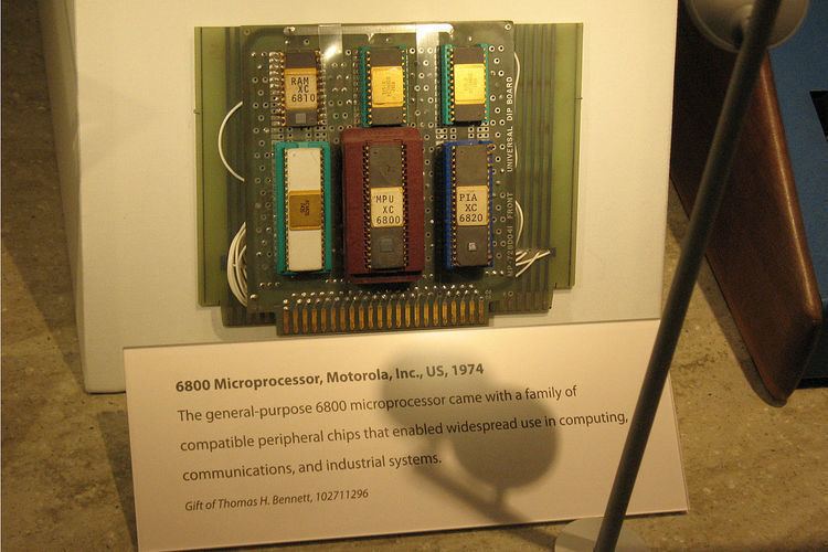
The 6502 was designed by many of the same engineers that had designed the Motorola 6800 microprocessor family. Motorola started the 6800 microprocessor project in 1971 with Tom Bennett as the main architect. The chip layout began in late 1972, the first 6800 chips were fabricated in February 1974 and the full family was officially released in November 1974. John Buchanan was the designer of the 6800 chip and Rod Orgill, who later did the 6501, assisted Buchanan with circuit analyses and chip layout. Bill Mensch joined Motorola in June 1971 after graduating from the University of Arizona (at age 26). His first assignment was helping define the peripheral ICs for the 6800 family and later he was the principal designer of the 6820 Peripheral Interface Adapter (PIA). Motorola's engineers could run analog and digital simulations on an IBM 370-165 mainframe computer. Bennett hired Chuck Peddle in 1973 to do architectural support work on the 6800 family products already in progress. He contributed in many areas including the design of the 6850 ACIA (serial interface).
Motorola's target customers were established electronics companies such as Hewlett-Packard, Tektronix, TRW and Chrysler. In May 1972 Motorola's engineers began visiting select customers and sharing the details of their proposed 8-bit microprocessor system with ROM, RAM, parallel and serial interfaces. In early 1974 they provided engineering samples of the chips so customers could prototype their designs. Motorola's "total product family" strategy did not focus on the price of the microprocessor but on reducing the customer's total design cost. They offered development software on a timeshare computer, the "EXORciser" system debugging system, onsite training and field application engineer support. Both Intel and Motorola had initially announced a $360 price for a single microprocessor. (The IBM System/360 mainframe was a well known computer at the time.) The actual price for production quantities was much less. Motorola offered a design kit containing the 6800 with six support chips for $300.
Peddle would accompany the sales people on customer visits and he found that customers were put off by the high cost of the microprocessor chips. To lower the price, the IC chip size would have to shrink so that more chips could be produced on each silicon wafer. This could be done by removing inessential features in the 6800 and using a newer fabrication technology, "depletion-mode" MOS transistors. Peddle and other team members started outlining the design of an improved feature, reduced size microprocessor. At that time Motorola's new semiconductor fabrication facility in Austin, Texas was having difficulty producing MOS chips and mid 1974 was the beginning of a year-long recession in the semiconductor industry. Also many of the Mesa, Arizona employees were displeased with the upcoming relocation to Austin. Motorola Semiconductor Products Division's management was overwhelmed with problems and showed no interest in Peddle's low-cost microprocessor proposal. Chuck Peddle was frustrated with Motorola's management for missing this new opportunity. In a November 1975 interview, Motorola's Chairman, Robert Galvin, agreed. He said, "We did not choose the right leaders in the Semiconductor Products division." The division was reorganized and the management replaced. New group vice-president, John Welty said, "The semiconductor sales organization lost its sensitivity to customer needs and couldn't make speedy decisions."
Peddle began looking for a source of funding for this new project and found a small semiconductor company in Pennsylvania. In August 1974, Chuck Peddle, Bill Mensch, Rod Orgill, Harry Bawcum, Ray Hirt, Terry Holdt and Wil Mathys left Motorola to join MOS Technology. (Mike James joined later.) Of the seventeen chip designers and layout people on the 6800 team, seven left. There were 30 to 40 other marketers, application engineers and system engineers on the 6800 team. That December, Gary Daniels transferred into the 6800 microprocessor group. Tom Bennett did not want to leave the Phoenix area so Daniels took over the microprocessor development in Austin. His first project was a "depletion-mode" version of the 6800; this cut the chip area nearly in half and doubled the speed. The faster parts were available in July 1976. This was followed by the 6802 which added 128 bytes of RAM and an on-chip clock oscillator circuit.
Moving to MOS Technology
MOS Technology was formed in 1969 by three executives from General Instrument, Mort Jaffe, Don McLaughlin, and John Pavinen, to produce metal-oxide-semiconductor (MOS) integrated circuits. Allen-Bradley, a supplier of electronic components and industrial controls, acquired a majority interest in 1970. The company designed and fabricated custom ICs for customers and had developed a line of calculator chips.
On August 19, 1974, the former Motorola employees moved into MOS Technology's headquarters at Valley Forge, Pennsylvania. The goal was to design and produce a low cost microprocessor for embedded applications and to target as wide as possible customer base. This would only be possible if the microprocessor was low cost – and in the semiconductor business, chip size determined cost. The size goal required n-channel "depletion-mode" MOS transistors, a more advanced process than MOS Technology's calculator chips used. John Pavinen was able to have the process ready by June 1975. Chuck Peddle, Rod Orgill, and Wil Mathys designed the initial architecture of the new processors. There would be two microprocessors: the 6501 would plug into the same socket as the Motorola 6800 while the 6502 would work with 6800 family peripherals and have an on-chip clock oscillator. These processors would not run 6800 software because they used a different instruction set. A September 1975 article in EDN magazine gives this summary of the design:
The MOS Technology 650X family represents a conscious attempt of eight former Motorola employees who worked on the development of the 6800 system to put out a part that would replace and outperform the 6800, yet undersell it. With the benefit of hindsight gained on the 6800 project, the MOS Technology team headed by Chuck Peddle, made the following architectural changes in the Motorola CPU…
The second "B" accumulator was omitted. The 16-bit 6800 index register was split into two 8-bit registers and these registers operate in the "true" indexing mode. Three-state control was eliminated from the address bus outputs. A clock generator was included on the chip. The address bus was always active so the VMA (valid-memory address) output was eliminated. An "8080-type" RDY signal for single-cycle stepping was added.
The chip high level design had to be turned into drawings of transistors and interconnects. At MOS Technology the "layout" was a very manual process done with color pencils and vellum paper. The layout consisted of thousands of polygon shapes on six different drawings; one for each layer of the semiconductor fabrication process. Rod Orgill was responsible for the 6501 design; he had assisted John Buchanan at Motorola on the 6800. Bill Mensch did the 6502; he was the designer of the 6820 Peripheral Interface Adapter (PIA) at Motorola. Harry Bawcom, Mike James and Sydney-Anne Holt helped with the layout.
The size goal for the 6502 chip was 153 x 168 mils (3.9 x 4.3 mm) or an area of 16.6 mm2. At that time the technical literature would state the length and width of each chip in "mils" (0.001 inch). The original 6800 chips were 212 x 212 mils (5.4 x 5.4 mm) or an area of 29.0 mm2. A smaller area means more chips per silicon wafer and those smaller chips were less likely to encounter a defect during fabrication. The first layouts did not reach their target size. The first 6502 chips were 168 x 183 mils (4.3 x 4.7 mm) or an area of 19.8 mm2. The Rotate Right instruction (ROR) did not work in the first silicon but the next iteration of the design shrank the chip and fixed the Rotate Right instruction.
Introducing the 6501 and 6502
MOS Technology's microprocessor introduction was quite different from the traditional months-long product launch. The first run of a new integrated circuit is normally used for internal testing and shared with select customers as "engineering samples." These chips often have a minor design defect or two that will be corrected before production begins. Chuck Peddle's goal was to sell the first run 6501 and 6502 chips to the attendees at the Wescon trade show in San Francisco beginning on September 16, 1975. Peddle was a very effective spokesman and the MOS Technology microprocessors were extensively covered in the trade press. One of the earliest was a full-page story on the MCS6501 and MCS6502 microprocessors in the July 24, 1975 issue of Electronics magazine. Stories also ran in EE Times (August 24, 1975), EDN (September 20, 1975), Electronic News (November 3, 1975), Byte (November 1975) and Microcomputer Digest (November 1975). Advertisements for the 6501 appeared in several publications the first week of August 1975. The 6501 would be for sale at Wescon for $20 each. In September 1975 the advertisements included both the 6501 and the 6502 microprocessors. The 6502 would cost only $25.
When MOS Technology arrived at Wescon, they found that exhibitors could not sell anything on the show floor. They rented the MacArthur Suite at the St. Francis Hotel and directed customers there to purchase the processors. At the suite the processors were stored in large jars to imply that the chips were in production and readily available. The customers did not know the bottom half of each jar contained non-functional chips. The chips were $20 and $25 while the documentation package was an additional $10. Users were encouraged to make copies of the documents, an inexpensive way for MOS Technology to distribute product information. The processors were supposed to have 56 instructions, but the Rotate Right (ROR) instruction did not work correctly on these chips, so the preliminary data sheets listed just 55 instructions. The reviews in Byte and EDN noted the lack of the ROR instruction. The next revision of the layout fixed this problem and the May 1976 datasheet listed 56 instructions. Peddle wanted every interested engineer and hobbyist to have access to the chips and documentation. Other semiconductor companies only wanted to deal with "serious" customers. For example, Signetics was introducing the 2650 microprocessor and its advertisements asked readers to write for information on their company letterhead.
Motorola lawsuit
The 6501/6502 introduction in print and at Wescon was an enormous success. The downside was the extensive press coverage got Motorola's attention. In October 1975, Motorola reduced the price of a single 6800 microprocessor from $175 to $69. The $300 system design kit was reduced to $150 and it now came with a printed circuit board. On November 3, 1975, Motorola sought an injunction in Federal Court to stop MOS Technology from making and selling microprocessor products. They also filed a lawsuit claiming patent infringement and misappropriation of trade secrets. Motorola claimed that seven former employees joined MOS Technology to create that company's microprocessor products.
Motorola was a billion-dollar company with a plausible case and lawyers. On October 30, 1974, Motorola had filed numerous patent applications on the microprocessor family and was granted twenty-five patents. The first was in June 1976 and the second was to Bill Mensch on July 6, 1976 for the 6820 PIA chip layout. These patents covered the 6800 bus and how the peripheral chips interfaced with the microprocessor. Motorola began making transistors in 1950 and had a portfolio of semiconductor patents. Allen-Bradley decided not to fight this case and sold their interest in MOS Technology back to the founders. Four of the former Motorola engineers were named in the suit: Chuck Peddle, Will Mathys, Bill Mensch and Rod Orgill. All were named inventors in the 6800 patent applications. During the discovery process, Motorola found that one engineer, Mike James, had ignored Peddle's instructions and brought his 6800 design documents to MOS Technology. In March 1976, the now independent MOS Technology was running out of money and had to settle the case. They agreed to drop the 6501 processor, pay Motorola $200,000 and return the documents that Motorola contended were confidential. Both companies agreed to cross-license microprocessor patents. That May, Motorola dropped the price of a single 6800 microprocessor to $35. By November Commodore had acquired MOS Technology.
Computers and games
With legal troubles behind them, MOS was still left with the problem of getting developers to try their processor, prompting Chuck Peddle to design the MDT-650 ("microcomputer development terminal") single-board computer. Another group inside the company designed the KIM-1, which was sold semi-complete and could be turned into a usable system with the addition of a 3rd party computer terminal and compact cassette drive. Much to their amazement, the KIM-1 sold well to hobbyists and tinkerers, as well as to the engineers to which it had been targeted. The related Rockwell AIM 65 control/training/development system also did well. The software in the AIM 65 was based on that in the MDT. Another roughly similar product was the Synertek SYM-1.
One of the first "public" uses for the design was the Apple I microcomputer, introduced in 1976. The 6502 was next used in the Commodore PET and the Apple II, both released in 1977. It was later used in the Atari home computers, the BBC Micro family, the Commodore VIC-20 and a large number of other designs both for home computers and business, such as Ohio Scientific and Oric. The 6510, a direct successor of the 6502 with a digital I/O port and a tri-state address bus, was the CPU utilized in the best-selling Commodore 64 home computer. Commodore's floppy disk drive, the 1541, had a processor of its own—it too was a 6502.
Another important use of the 6500 family was in video games. The first to make use of the processor design was the Atari 2600 video game console. The 2600 used an offshoot of the 6502 called the 6507, which had fewer pins and, as a result, could address only 8 KB of memory. Millions of the Atari consoles would be sold, each with a MOS processor. Another significant use was by the Nintendo Entertainment System and Famicom. The 6502 used in the NES was a second source version by Ricoh, a partial system-on-a-chip, that lacked the binary-coded decimal mode but added 22 memory-mapped registers (and on-die hardware) for sound generation, joypad reading, and sprite list DMA. Called 2A03 in NTSC consoles and 2A07 in PAL consoles (the difference being the memory divider ratio and a lookup table for audio sample rates), this processor was produced exclusively for Nintendo.
In the 1980s a popular electronics magazine Elektor/Elektuur used the processor in its microprocessor development board Junior Computer.
Technical description
The 6502 is a little-endian 8-bit processor with a 16-bit address bus. The original versions were fabricated using an 8 µm process technology chip with an advertised die size of 153 x 168 mils (3.9 x 4.3 mm) or an area of 16.6 mm2.
The internal logic runs at the same speed as the external clock rate, but despite the slow clock speeds (typically in the neighborhood of 1 to 2 MHz), the 6502's performance was competitive with other contemporary CPUs using significantly faster clocks. This is partly due to a simplistic state machine implemented by combinatorial (clockless) logic to a greater extent than in many other designs; the two phase clock (supplying two synchronizations per cycle) can thereby control the whole machine-cycle directly. Typical instructions might take half as many cycles to complete on the 6502 than contemporary designs. Like most simple CPUs of the era, the dynamic NMOS 6502 chip is not sequenced by a microcode ROM but uses a PLA (which occupied about 15 percent of the chip area) for instruction decoding and sequencing. Like most eight-bit microprocessors, the chip does some limited overlapping of fetching and execution.
The low clock frequency moderated the speed requirement of memory and peripherals attached to the CPU, as only about 50 percent of the clock cycle was available for memory access (due to the asynchronous design, this percentage varied strongly among chip versions). This was critical at a time when affordable memory had access times in the range 250 - 450 ns. The original NMOS 6502 was minimalistically engineered and efficiently manufactured and therefore cheap—an important factor in getting design wins in the very price-sensitive game console and home computer markets. Like its precursor, the Motorola 6800, the 6502 has very few registers. At the time the processor was designed, the number of transistors that could be economically put on a chip was very constrained (around a few thousand), so it made sense to rely on RAM instead of allocating expensive NMOS chip area for CPU registers.
Registers
The 6502's registers include one 8-bit accumulator register (A), two 8-bit index registers (X and Y), 7 processor status flag bits (P), an 8-bit stack pointer (S), and a 16-bit program counter (PC). The stack's address space is hardwired to memory page $01, i.e. the address range $0100–$01FF (256–511). Software access to the stack is done via four implied addressing mode instructions, whose functions are to push or pop (pull) the accumulator or the processor status register. The same stack is also used for subroutine calls via the JSR (Jump to Subroutine) and RTS (Return from Subroutine) instructions and for interrupt handling.
Addressing
The chip uses the index and stack registers effectively with several addressing modes, including a fast "direct page" or "zero page" mode, similar to that found on the PDP-8, that accesses memory locations from addresses 0 to 255 with a single 8-bit address (saving the cycle normally required to fetch the high-order byte of the address)—code for the 6502 uses the zero page much as code for other processors would use registers. On some 6502-based microcomputers with an operating system, the OS uses most of zero page, leaving only a handful of locations for the user.
Addressing modes also include implied (1 byte instructions); absolute (3 bytes); indexed absolute (3 bytes); indexed zero-page (2 bytes); relative (2 bytes); accumulator (1); indirect,x and indirect,y (2); and immediate (2). Absolute mode is a general-purpose mode. Branch instructions use a signed 8-bit offset relative to the instruction after the branch; the numerical range -128..127 therefore translates to 128 bytes backward and 127 bytes forward from the instruction following the branch (which is 126 bytes backward and 129 bytes forward from the start of the branch instruction). Accumulator mode uses the accumulator as an effective address, and does not need any operand data. Immediate mode uses an 8-bit literal operand.
Indirect addressing
The indirect modes are useful for array processing and other looping. With the 5/6 cycle "(indirect),y" mode, the 8-bit Y register is added to a 16-bit base address read from zero page which is located by a single byte following the opcode. The Y register is therefore an index-register in the sense that it is used to hold an actual index (as opposed to the X register in the 6800 where a base address was directly stored and to which an immediate offset could be added). Incrementing the index register to walk the array byte-wise takes only two additional cycles. With the less frequently used "(indirect,x)" mode the effective address for the operation is found at the zero page address formed by adding the second byte of the instruction to the contents of the X register. Using the indexed modes, the zero page effectively acts as a set of up to 128 additional (though very slow) address registers.
The 6502 is capable of performing addition and subtraction in binary or binary coded decimal. Placing the CPU into BCD mode with the SED (set D flag) instruction results in decimal arithmetic, in which $99 + $01 would result in $00 and the carry (C) flag being set. In binary mode (CLD, clear D flag), the same operation would result in $9A and the carry flag being cleared. Other than Atari BASIC, BCD mode was seldom used in home computer applications.
See the Hello world! article for a simple but characteristic example of 6502 assembly language.
Detailed behavior
The processor's non-maskable interrupt (NMI) input is edge sensitive, which means that the interrupt is triggered by the falling edge of the signal rather than its level. The implication of this feature is that a wired-OR interrupt circuit is not readily supported. However, this also prevents nested NMI interrupts from occurring until the hardware makes the NMI input inactive again, often under control of the NMI interrupt handler.
The simultaneous assertion of the NMI and IRQ (maskable) hardware interrupt lines causes IRQ to be ignored. However, if the IRQ line remains asserted after the servicing of the NMI, the processor will immediately respond to IRQ, as IRQ is level sensitive. Thus a sort of built-in interrupt priority was established in the 6502 design.
The "Break" flag of the processor is very different from the other flag bits. It has no flag setting, resetting, and testing instructions of its own, and is not affected by the PHP and PLP instructions. It exists only on the stack, where BRK and PHP always write a 1, while IRQ and NMI always write a 0.
The "SO" input pin, when asserted, will set the processor's overflow status bit (deasserting it does not clear the overflow bit, however). This can be used by a high-speed polling device driver, which can poll the hardware once in only three cycles by using a Branch-on-oVerflow-Clear (BVC) instruction that branches to itself. For example, the Commodore 1541 and other Commodore floppy disk drives use this technique to detect without delay whether the serializer is ready to accept or provide another byte of disk data. Obviously great care must be used in the device driver and the associated system design, as spurious assertion of the overflow bit could ruin arithmetic processing.
Assembly language instructions
A 6502 assembly language statement consists of a three character instruction mnemonic, followed by an operand in the case of an instruction that takes an operand. When assembled, the resulting machine code will consist of a one byte operation code (opcode), followed by a one or two byte operand, if the instruction was assembled with an operand, hence 6502 machine instructions vary in length from one to three bytes. The operand will be stored in the 6502's customary little-endian format. The 65C816, the 16-bit CMOS version of the 6502, also supports 24 bit addressing, which addressing modes will result in instructions being assembled with three byte operands, also arranged in little-endian format.
Variations and derivatives
There were several variants of the NMOS 6502:
6512
The MOS Technology 6512 relies on an external clock, instead of using an internal clock generator like the 6502. This was used to advantage in some designs where the clocks could be run asymmetrically, increasing overall CPU performance.
The 6512 was used in the BBC Micro B+64.
16-bit derivatives
The Western Design Center designed and currently produces the W65C816S processor, a 16-bit, static-core successor to the 65C02, with greatly enhanced features. The 65C816 powered the Apple IIGS computer, and was the basis of the Ricoh 5A22 processor that powered the popular Super Nintendo Entertainment System. The W65C816S is available through electronics distributors.
The Western Design Center also designed and produced the 65C802, which was a 65C816 core with a 64 KB address space in a 65(C)02 pin-compatible package. The 65C802 could be retrofitted to a 6502 board and would function as a 65C02 on power-up, operating in "emulation mode." As with the 65C816, a two-instruction sequence would switch the 65C802 to "native mode" operation, exposing its 16 bit accumulator and index registers, as well as other 65C816 enhanced features. The 65C802 was not widely used—new designs almost always were built around the 65C816, resulting in 65C802 production being discontinued.
32-bit derivatives
The 65GZ032 designed by Gideon Zweijtzer is a VHDL source core that is 6502 compatible and extends the 8-bit CPU to a 32-bit design. It features pipelined RISC, new opcodes, access to 4 GByte of linear memory, paged memory and a clock speed of 33 MHz.
Example code
The following 6502 assembly language source code is for a subroutine named TOLOWER, which copies a null-terminated character string from one location to another, converting upper case letter characters to lower case letters. The string being copied is the "source" and the string into which the converted source is stored is the "destination."
Bugs and quirks
Acceleration
As the 6502 is externally clocked, upgrading the speed involves more than dropping a faster chip into the processor socket; many other components also need to be modified. To meet user demand, a number of companies sold hardware to speed up those systems. These "accelerators" included a modicum of high-speed RAM and glue circuitry used to synchronize the faster processor with the computer's original RAM and its peripherals. For example, the Apple II floppy disk relied on software accessing the controller's I/O registers with critical timing; Apple II accelerators were therefore designed to fall back to 1 MHz during disk access. The first accelerators were circuit boards; some later accelerators (such as the Zip Chip) miniaturized the processor and support circuits to fit into a DIP package that was plug compatible with the original processor.