
 | ||
A bipolar junction transistor (bipolar transistor or BJT) is a type of transistor that uses both electron and hole charge carriers. In contrast, unipolar transistors, such as field-effect transistors, only use one kind of charge carrier. For their operation, BJTs use two junctions between two semiconductor types, n-type and p-type.
Contents
- Note on current direction
- Function
- Voltage current and charge control
- Turn on turn off and storage delay
- Transistor parameters alpha and beta
- Structure
- NPN
- PNP
- Heterojunction bipolar transistor
- Regions of operation
- Active mode NPN transistors in circuits
- Active mode PNP transistors in circuits
- History
- Germanium transistors
- Early manufacturing techniques
- Bipolar transistors
- Theory and modeling
- Large signal models
- EbersMoll model
- GummelPoon charge control model
- hybrid pi model
- h parameter model
- Industry models
- Applications
- High speed digital logic
- Amplifiers
- Temperature sensors
- Logarithmic converters
- Vulnerabilities
- References
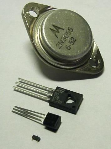
BJTs are manufactured in two types, NPN and PNP, and are available as individual components, or fabricated in integrated circuits, often in large numbers. The basic function of a BJT is to amplify current. This allows BJTs to be used as amplifiers or switches, giving them wide applicability in electronic equipment, including computers, televisions, mobile phones, audio amplifiers, industrial control, and radio transmitters.
Note on current direction
By convention, the direction of current on diagrams is shown as the direction that a positive charge would move. This is called conventional current. However, current in many metal conductors is due to the flow of electrons which, because they carry a negative charge, move in the opposite direction to conventional current. On the other hand, inside a bipolar transistor, currents can be composed of both positively charged holes and negatively charged electrons. In this article, current arrows are shown in the conventional direction, but labels for the movement of holes and electrons show their actual direction inside the transistor. The arrow on the symbol for bipolar transistors points in the direction conventional current travels.
Function
BJTs come in two types, or polarities, known as PNP and NPN based on the doping types of the three main terminal regions. An NPN transistor comprises two semiconductor junctions that share a thin p-doped region, and a PNP transistor comprises two semiconductor junctions that share a thin n-doped region.
Charge flow in a BJT is due to diffusion of charge carriers across a junction between two regions of different charge concentrations. The regions of a BJT are called emitter, collector, and base. A discrete transistor has three leads for connection to these regions. Typically, the emitter region is heavily doped compared to the other two layers, whereas the majority charge carrier concentrations in base and collector layers are about the same. By design, most of the BJT collector current is due to the flow of charges injected from a high-concentration emitter into the base where they are minority carriers that diffuse toward the collector, and so BJTs are classified as minority-carrier devices.
In typical operation, the base–emitter junction is forward biased, which means that the p-doped side of the junction is at a more positive potential than the n-doped side, and the base–collector junction is reverse biased. In an NPN transistor, when positive bias is applied to the base–emitter junction, the equilibrium is disturbed between the thermally generated carriers and the repelling electric field of the n-doped emitter depletion region. This allows thermally excited electrons to inject from the emitter into the base region. These electrons diffuse through the base from the region of high concentration near the emitter towards the region of low concentration near the collector. The electrons in the base are called minority carriers because the base is doped p-type, which makes holes the majority carrier in the base.
To minimize the percentage of carriers that recombine before reaching the collector–base junction, the transistor's base region must be thin enough that carriers can diffuse across it in much less time than the semiconductor's minority carrier lifetime. In particular, the thickness of the base must be much less than the diffusion length of the electrons. The collector–base junction is reverse-biased, and so little electron injection occurs from the collector to the base, but electrons that diffuse through the base towards the collector are swept into the collector by the electric field in the depletion region of the collector–base junction. The thin shared base and asymmetric collector–emitter doping are what differentiates a bipolar transistor from two separate and oppositely biased diodes connected in series.
Voltage, current, and charge control
The collector–emitter current can be viewed as being controlled by the base–emitter current (current control), or by the base–emitter voltage (voltage control). These views are related by the current–voltage relation of the base–emitter junction, which is just the usual exponential current–voltage curve of a p-n junction (diode).
The physical explanation for collector current is the concentration of minority carriers in the base region. Due to low level injection (in which there are much fewer excess carriers than normal majority carriers) the ambipolar transport rates (in which the excess majority and minority carriers flow at the same rate) is in effect determined by the excess minority carriers.
Detailed transistor models of transistor action, such as the Gummel–Poon model, account for the distribution of this charge explicitly to explain transistor behaviour more exactly. The charge-control view easily handles phototransistors, where minority carriers in the base region are created by the absorption of photons, and handles the dynamics of turn-off, or recovery time, which depends on charge in the base region recombining. However, because base charge is not a signal that is visible at the terminals, the current- and voltage-control views are generally used in circuit design and analysis.
In analog circuit design, the current-control view is sometimes used because it is approximately linear. That is, the collector current is approximately
Turn-on, turn-off, and storage delay
The bipolar transistor exhibits a few delay characteristics when turning on and off. Most transistors, and especially power transistors, exhibit long base-storage times that limit maximum frequency of operation in switching applications. One method for reducing this storage time is by using a Baker clamp.
Transistor parameters: alpha (α) and beta (β)
The proportion of electrons able to cross the base and reach the collector is a measure of the BJT efficiency. The heavy doping of the emitter region and light doping of the base region causes many more electrons to be injected from the emitter into the base than holes to be injected from the base into the emitter.
The common-emitter current gain is represented by βF or the h-parameter hFE; it is approximately the ratio of the DC collector current to the DC base current in forward-active region. It is typically greater than 50 for small-signal transistors but can be smaller in transistors designed for high-power applications.
Another important parameter is the common-base current gain, αF. The common-base current gain is approximately the gain of current from emitter to collector in the forward-active region. This ratio usually has a value close to unity; between 0.980 and 0.998. It is less than unity due to recombination of charge carriers as they cross the base region.
Alpha and beta are more precisely related by the following identities (NPN transistor):
Structure
A BJT consists of three differently doped semiconductor regions: the emitter region, the base region and the collector region. These regions are, respectively, p type, n type and p type in a PNP transistor, and n type, p type and n type in an NPN transistor. Each semiconductor region is connected to a terminal, appropriately labeled: emitter (E), base (B) and collector (C).
The base is physically located between the emitter and the collector and is made from lightly doped, high-resistivity material. The collector surrounds the emitter region, making it almost impossible for the electrons injected into the base region to escape without being collected, thus making the resulting value of α very close to unity, and so, giving the transistor a large β. A cross-section view of a BJT indicates that the collector–base junction has a much larger area than the emitter–base junction.
The bipolar junction transistor, unlike other transistors, is usually not a symmetrical device. This means that interchanging the collector and the emitter makes the transistor leave the forward active mode and start to operate in reverse mode. Because the transistor's internal structure is usually optimized for forward-mode operation, interchanging the collector and the emitter makes the values of α and β in reverse operation much smaller than those in forward operation; often the α of the reverse mode is lower than 0.5. The lack of symmetry is primarily due to the doping ratios of the emitter and the collector. The emitter is heavily doped, while the collector is lightly doped, allowing a large reverse bias voltage to be applied before the collector–base junction breaks down. The collector–base junction is reverse biased in normal operation. The reason the emitter is heavily doped is to increase the emitter injection efficiency: the ratio of carriers injected by the emitter to those injected by the base. For high current gain, most of the carriers injected into the emitter–base junction must come from the emitter.
The low-performance "lateral" bipolar transistors sometimes used in CMOS processes are sometimes designed symmetrically, that is, with no difference between forward and backward operation.
Small changes in the voltage applied across the base–emitter terminals cause the current between the emitter and the collector to change significantly. This effect can be used to amplify the input voltage or current. BJTs can be thought of as voltage-controlled current sources, but are more simply characterized as current-controlled current sources, or current amplifiers, due to the low impedance at the base.
Early transistors were made from germanium but most modern BJTs are made from silicon. A significant minority are also now made from gallium arsenide, especially for very high speed applications (see HBT, below).
NPN
NPN is one of the two types of bipolar transistors, consisting of a layer of P-doped semiconductor (the "base") between two N-doped layers. A small current entering the base is amplified to produce a large collector and emitter current. That is, when there is a positive potential difference measured from the base of an NPN transistor to its emitter (that is, when the base is high relative to the emitter), as well as a positive potential difference measured from the collector to the emitter, the transistor becomes active. In this "on" state, charge flows from the collector to the emitter of the transistor. Most of the current is carried by electrons moving from emitter to collector as minority carriers in the P-type base region. To allow for greater current and faster operation, most bipolar transistors used today are NPN because electron mobility is higher than hole mobility.
A mnemonic device for the NPN transistor symbol is "not pointing in", based on the arrows in the symbol and the letters in the name.
PNP
The other type of BJT is the PNP, consisting of a layer of N-doped semiconductor between two layers of P-doped material. A small current leaving the base is amplified in the collector output. That is, a PNP transistor is "on" when its base is pulled low relative to the emitter. In a PNP transistor, the emitter–base region is forward biased, so holes are injected into the base as minority carriers. The base is very thin, and most of the holes cross the reverse-biased base–collector junction to the collector.
The arrows in the NPN and PNP transistor symbols are on the emitter legs and point in the direction of the conventional current when the device is in forward active or forward saturated mode.
A mnemonic device for the PNP transistor symbol is "pointing in (proudly/permanently)", based on the arrows in the symbol and the letters in the name.
Heterojunction bipolar transistor
The heterojunction bipolar transistor (HBT) is an improvement of the BJT that can handle signals of very high frequencies up to several hundred GHz. It is common in modern ultrafast circuits, mostly RF systems.
Heterojunction transistors have different semiconductors for the elements of the transistor. Usually the emitter is composed of a larger bandgap material than the base. The figure shows that this difference in bandgap allows the barrier for holes to inject backward from the base into the emitter, denoted in the figure as Δφp, to be made large, while the barrier for electrons to inject into the base Δφn is made low. This barrier arrangement helps reduce minority carrier injection from the base when the emitter-base junction is under forward bias, and thus reduces base current and increases emitter injection efficiency.
The improved injection of carriers into the base allows the base to have a higher doping level, resulting in lower resistance to access the base electrode. In the more traditional BJT, also referred to as homojunction BJT, the efficiency of carrier injection from the emitter to the base is primarily determined by the doping ratio between the emitter and base, which means the base must be lightly doped to obtain high injection efficiency, making its resistance relatively high. In addition, higher doping in the base can improve figures of merit like the Early voltage by lessening base narrowing.
The grading of composition in the base, for example, by progressively increasing the amount of germanium in a SiGe transistor, causes a gradient in bandgap in the neutral base, denoted in the figure by ΔφG, providing a "built-in" field that assists electron transport across the base. That drift component of transport aids the normal diffusive transport, increasing the frequency response of the transistor by shortening the transit time across the base.
Two commonly used HBTs are silicon–germanium and aluminum gallium arsenide, though a wide variety of semiconductors may be used for the HBT structure. HBT structures are usually grown by epitaxy techniques like MOCVD and MBE.
Regions of operation
Bipolar transistors have four distinct regions of operation, defined by BJT junction biases.
The modes of operation can be described in terms of the applied voltages (this description applies to NPN transistors; polarities are reversed for PNP transistors):
In terms of junction biasing: (reverse biased base–collector junction means Vbc < 0 for NPN, opposite for PNP)
Although these regions are well defined for sufficiently large applied voltage, they overlap somewhat for small (less than a few hundred millivolts) biases. For example, in the typical grounded-emitter configuration of an NPN BJT used as a pulldown switch in digital logic, the "off" state never involves a reverse-biased junction because the base voltage never goes below ground; nevertheless the forward bias is close enough to zero that essentially no current flows, so this end of the forward active region can be regarded as the cutoff region.
Active-mode NPN transistors in circuits
The diagram shows a schematic representation of an NPN transistor connected to two voltage sources. To make the transistor conduct appreciable current (on the order of 1 mA) from C to E, VBE must be above a minimum value sometimes referred to as the cut-in voltage. The cut-in voltage is usually about 650 mV for silicon BJTs at room temperature but can be different depending on the type of transistor and its biasing. This applied voltage causes the lower P-N junction to 'turn on', allowing a flow of electrons from the emitter into the base. In active mode, the electric field existing between base and collector (caused by VCE) will cause the majority of these electrons to cross the upper P-N junction into the collector to form the collector current IC. The remainder of the electrons recombine with holes, the majority carriers in the base, making a current through the base connection to form the base current, IB. As shown in the diagram, the emitter current, IE, is the total transistor current, which is the sum of the other terminal currents, (i.e., IE = IB + IC).
In the diagram, the arrows representing current point in the direction of conventional current – the flow of electrons is in the opposite direction of the arrows because electrons carry negative electric charge. In active mode, the ratio of the collector current to the base current is called the DC current gain. This gain is usually 100 or more, but robust circuit designs do not depend on the exact value (for example see op-amp). The value of this gain for DC signals is referred to as
The emitter current is related to
Active-mode PNP transistors in circuits
The diagram shows a schematic representation of a PNP transistor connected to two voltage sources. To make the transistor conduct appreciable current (on the order of 1 mA) from E to C,
In the diagram, the arrows representing current point in the direction of conventional current – the flow of holes is in the same direction of the arrows because holes carry positive electric charge. In active mode, the ratio of the collector current to the base current is called the DC current gain. This gain is usually 100 or more, but robust circuit designs do not depend on the exact value. The value of this gain for DC signals is referred to as
The emitter current is related to
History
The bipolar point-contact transistor was invented in December 1947 at the Bell Telephone Laboratories by John Bardeen and Walter Brattain under the direction of William Shockley. The junction version known as the bipolar junction transistor (BJT), invented by Shockley in 1948, was for three decades the device of choice in the design of discrete and integrated circuits. Nowadays, the use of the BJT has declined in favor of CMOS technology in the design of digital integrated circuits. The incidental low performance BJTs inherent in CMOS ICs, however, are often utilized as bandgap voltage reference, silicon bandgap temperature sensor and to handle electrostatic discharge.
Germanium transistors
The germanium transistor was more common in the 1950s and 1960s, and while it exhibits a lower "cut-off" voltage, typically around 0.2 V, making it more suitable for some applications, it also has a greater tendency to exhibit thermal runaway.
Early manufacturing techniques
Various methods of manufacturing bipolar transistors were developed.
Bipolar transistors
Theory and modeling
Transistors can be thought of as two diodes (P–N junctions) sharing a common region that minority carriers can move through. A PNP BJT will function like two diodes that share an N-type cathode region, and the NPN like two diodes sharing a P-type anode region. Connecting two diodes with wires will not make a transistor, since minority carriers will not be able to get from one P–N junction to the other through the wire.
Both types of BJT function by letting a small current input to the base control an amplified output from the collector. The result is that the transistor makes a good switch that is controlled by its base input. The BJT also makes a good amplifier, since it can multiply a weak input signal to about 100 times its original strength. Networks of transistors are used to make powerful amplifiers with many different applications. In the discussion below, focus is on the NPN bipolar transistor. In the NPN transistor in what is called active mode, the base–emitter voltage
Large-signal models
In 1954, Jewell James Ebers and John L. Moll introduced their mathematical model of transistor currents:
Ebers–Moll model
The DC emitter and collector currents in active mode are well modeled by an approximation to the Ebers–Moll model:
The base internal current is mainly by diffusion (see Fick's law) and
where
The
The unapproximated Ebers–Moll equations used to describe the three currents in any operating region are given below. These equations are based on the transport model for a bipolar junction transistor.
where
Base-width modulation
As the collector–base voltage (
Narrowing of the base width has two consequences:
Both factors increase the collector or "output" current of the transistor in response to an increase in the collector–base voltage.
In the forward-active region, the Early effect modifies the collector current (
where:
Punchthrough
When the base–collector voltage reaches a certain (device-specific) value, the base–collector depletion region boundary meets the base–emitter depletion region boundary. When in this state the transistor effectively has no base. The device thus loses all gain when in this state.
Gummel–Poon charge-control model
The Gummel–Poon model is a detailed charge-controlled model of BJT dynamics, which has been adopted and elaborated by others to explain transistor dynamics in greater detail than the terminal-based models typically do. This model also includes the dependence of transistor
hybrid-pi model
The hybrid-pi model is a popular circuit model used for analyzing the small signal behavior of bipolar junction and field effect transistors. Sometimes it is also called Giacoletto model because it was introduced by L.J. Giacoletto in 1969. The model can be quite accurate for low-frequency circuits and can easily be adapted for higher-frequency circuits with the addition of appropriate inter-electrode capacitances and other parasitic elements.
h-parameter model
Another model commonly used to analyze BJT circuits is the h-parameter model, closely related to the hybrid-pi model and the y-parameter two-port, but using input current and output voltage as independent variables, rather than input and output voltages. This two-port network is particularly suited to BJTs as it lends itself easily to the analysis of circuit behaviour, and may be used to develop further accurate models. As shown, the term, x, in the model represents a different BJT lead depending on the topology used. For common-emitter mode the various symbols take on the specific values as:
and the h-parameters are given by:
As shown, the h-parameters have lower-case subscripts and hence signify AC conditions or analyses. For DC conditions they are specified in upper-case. For the CE topology, an approximate h-parameter model is commonly used which further simplifies the circuit analysis. For this the hoe and hre parameters are neglected (that is, they are set to infinity and zero, respectively). The h-parameter model as shown is suited to low-frequency, small-signal analysis. For high-frequency analyses the inter-electrode capacitances that are important at high frequencies must be added.
Etymology of hFE
The h refers to its being an h-parameter, a set of parameters named for their origin in a hybrid equivalent circuit model. F is from forward current amplification also called the current gain. E refers to the transistor operating in a common emitter (CE) configuration. Capital letters used in the subscript indicate that hFE refers to a direct current circuit.
Industry models
The Gummel–Poon SPICE model is often used, but it suffers from several limitations. These have been addressed in various more advanced models: Mextram, VBIC, HICUM, Modella.
Applications
The BJT remains a device that excels in some applications, such as discrete circuit design, due to the very wide selection of BJT types available, and because of its high transconductance and output resistance compared to MOSFETs.
The BJT is also the choice for demanding analog circuits, especially for very-high-frequency applications, such as radio-frequency circuits for wireless systems.
High speed digital logic
Emitter-coupled logic (ECL) use BJTs.
Bipolar transistors can be combined with MOSFETs in an integrated circuit by using a BiCMOS process of wafer fabrication to create circuits that take advantage of the application strengths of both types of transistor.
Amplifiers
The transistor parameters α and β characterizes the current gain of the BJT. It is this gain that allows BJTs to be used as the building blocks of electronic amplifiers. The three main BJT amplifier topologies are:
Temperature sensors
Because of the known temperature and current dependence of the forward-biased base–emitter junction voltage, the BJT can be used to measure temperature by subtracting two voltages at two different bias currents in a known ratio.
Logarithmic converters
Because base–emitter voltage varies as the logarithm of the base–emitter and collector–emitter currents, a BJT can also be used to compute logarithms and anti-logarithms. A diode can also perform these nonlinear functions but the transistor provides more circuit flexibility.
Vulnerabilities
Exposure of the transistor to ionizing radiation causes radiation damage. Radiation causes a buildup of 'defects' in the base region that act as recombination centers. The resulting reduction in minority carrier lifetime causes gradual loss of gain of the transistor.
Power BJTs are subject to a failure mode called secondary breakdown, in which excessive current and normal imperfections in the silicon die cause portions of the silicon inside the device to become disproportionately hotter than the others. The electrical resistivity of doped silicon, like other semiconductors, has a negative temperature coefficient, meaning that it conducts more current at higher temperatures. Thus, the hottest part of the die conducts the most current, causing its conductivity to increase, which then causes it to become progressively hotter again, until the device fails internally. The thermal runaway process associated with secondary breakdown, once triggered, occurs almost instantly and may catastrophically damage the transistor package.
If the emitter-base junction is reverse biased into avalanche or Zener mode and charge flows for a short period of time, the current gain of the BJT will be permanently degraded.