
 | ||
The Early effect, named after its discoverer James M. Early, is the variation in the width of the base in a bipolar junction transistor (BJT) due to a variation in the applied base-to-collector voltage. A greater reverse bias across the collector–base junction, for example, increases the collector–base depletion width, decreasing the width of the charge carrier portion of the base.
Contents
Explanation
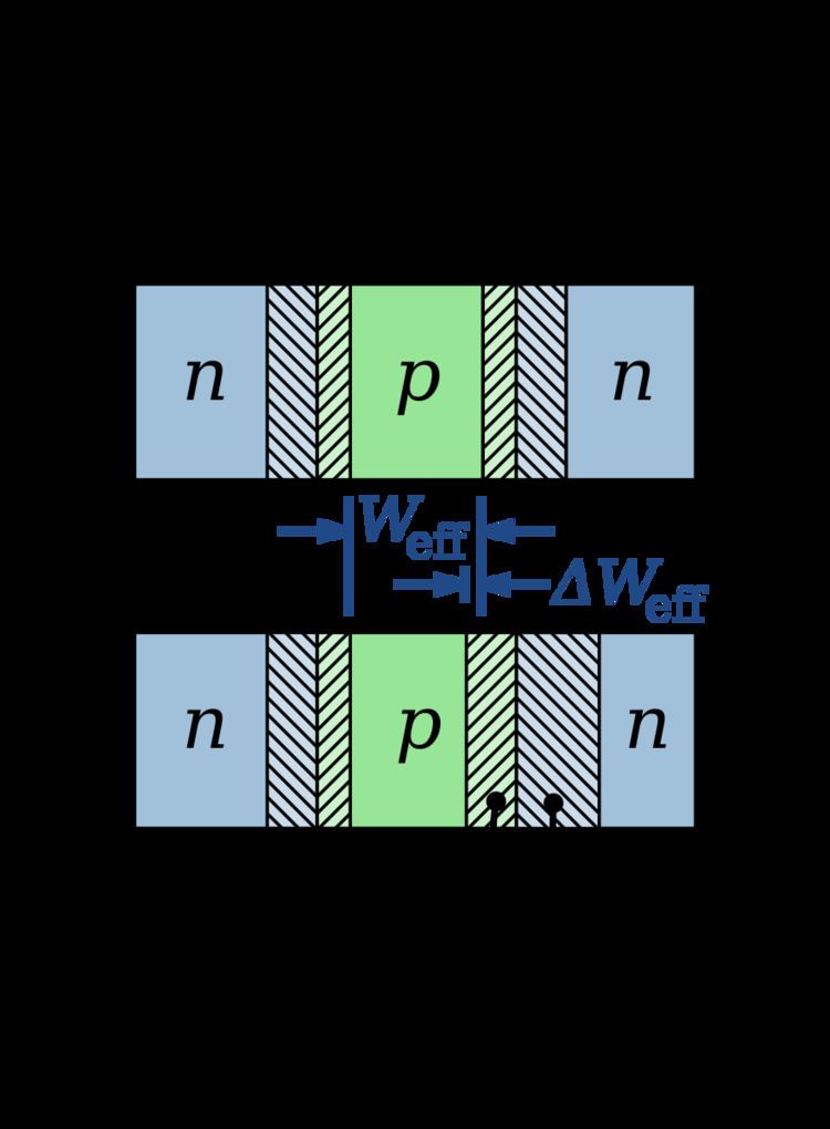
In Figure 1, the neutral (i.e. active) base is green, and the depleted base regions are hashed light green. The neutral emitter and collector regions are dark blue and the depleted regions hashed light blue. Under increased collector–base reverse bias, the lower panel of Figure 1 shows a widening of the depletion region in the base and the associated narrowing of the neutral base region.
The collector depletion region also increases under reverse bias, more than does that of the base, because the collector is less heavily doped. The principle governing these two widths is charge neutrality. The narrowing of the collector does not have a significant effect as the collector is much longer than the base. The emitter–base junction is unchanged because the emitter–base voltage is the same.
Base-narrowing has two consequences that affect the current:
Both these factors increase the collector or "output" current of the transistor with an increase in the collector voltage, but only the second is called Early effect. This increased current is shown in Figure 2. Tangents to the characteristics at large voltages extrapolate backward to intercept the voltage axis at a voltage called the Early voltage, often denoted by the symbol VA.
Large-signal model of the transistor
In the forward active region the Early effect modifies the collector current (
Where
Some models base the collector current correction factor on the collector–base voltage VCB (as described in base-width modulation) instead of the collector–emitter voltage VCE. Using VCB may be more physically plausible, in agreement with the physical origin of the effect, which is a widening of the collector–base depletion layer that depends on VCB. Computer models such as those used in SPICE use the collector–base voltage VCB.
Small-signal model
The Early effect can be accounted for in small-signal circuit models (such as the hybrid-pi model) as a resistor defined as
in parallel with the collector–emitter junction of the transistor. This resistor can thus account for the finite output resistance of a simple current mirror or an actively loaded common-emitter amplifier.
In keeping with the model used in SPICE and as discussed above using
which almost agrees with the textbook result. In either formulation,
In the MOSFET the output resistance is given in Shichman–Hodges model (accurate for very old technology) as:
where
Current–voltage characteristics
The expressions are derived for a PNP transistor. For an NPN transistor, n has to be replaced by p, and p has to be replaced by n in all expressions below. The following assumptions are involved when deriving ideal current-voltage characteristics of the BJT
It is important to characterize the minority diffusion currents induced by injection of carriers.
With regard to pn-junction diode, a key relation is the diffusion equation.
A solution of this equation is below, and two boundary conditions are used to solve and find
The following equations apply to the emitter and collector region, respectively, and the origins
A boundary condition of the emitter is below:
The values of the constants
Because
Expressions of
Because insignificant recombination occurs, the second derivative of
The following are boundary conditions of
with W the base width. Substitute into the above linear relation.
With this result, derive value of
Use the expressions of
Similarly, an expression of the collector current is derived.
An expression of the base current is found with the previous results.