
 | ||
The grown-junction transistor was the first type of bipolar junction transistor made. It was invented by William Shockley at Bell Labs on June 23, 1948 (patent filed June 26, 1948), six months after the first bipolar point-contact transistor. The first germanium prototypes were made in 1949. Bell Labs announced Shockley’s grown-junction transistor on July 4, 1951.
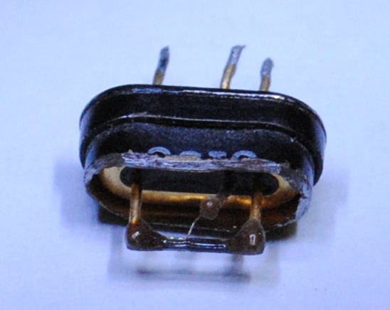
An NPN grown-junction transistor is made of a single crystal of semiconductor material which has two PN junctions grown into it. During the growth process, a seed crystal is slowly pulled from a bath of molten semiconductor, which then grows into a rod-shaped crystal (boule). The molten semiconductor is doped N-type at the start. At a predetermined moment in the growth process a small pellet of a P-type dopant is added, almost immediately followed by a somewhat larger pellet of an N-type dopant. These dopants dissolve in the molten semiconductor changing the type of semiconductor subsequently grown. The resulting crystal has a thin layer of P-type material sandwiched between sections of N-type material. This P-type layer may be as little as a thousandth of an inch thick. The crystal is sliced, leaving the thin P-type layer in the center of the slice, then cut into bars. Each bar is made into a transistor by soldering its N-type ends to supporting and conducting leads, then welding a very fine gold lead to the central P-type layer, and finally encasing in a hermetically sealed can. A similar process, using the opposite dopants, makes a PNP grown-junction transistor.
The most difficult part of this process is welding the gold wire to the base layer, as the wire may have a larger diameter than the thickness of the base. To facilitate this operation, the gold wire is pointed or flattened until the end is thinner than the base layer. The tip of the gold wire is slid along the bar until electrical resistance measurement shows it is in contact with the base layer. At this time a pulse of current is applied, welding the wire in place. Unfortunately sometimes the weld is too large or slightly off center in the base layer. To avoid shorting the transistor, the gold wire is alloyed with a small amount of the same type dopant as used in the base. This causes the base layer to become slightly thicker at the point of the weld.
Grown-junction transistors rarely operated at frequencies above the audio range, due to their relatively thick base layers. Growing thin base layers was very hard to control and welding the wire to the base became harder the thinner it got. Higher-frequency operation could be obtained by welding a second wire on the opposite side of the base, making a tetrode transistor, and using special biasing on this second base connection.