
 | ||
Surface states are electronic states found at the surface of materials. They are formed due to the sharp transition from solid material that ends with a surface and are found only at the atom layers closest to the surface. The termination of a material with a surface leads to a change of the electronic band structure from the bulk material to the vacuum. In the weakened potential at the surface, new electronic states can be formed, so called surface states.
Contents
- Origin of surface states at condensed matter interfaces
- Shockley states and Tamm states
- Topological surface states
- Surface states in metals
- Surface states in semiconductors
- Surface states of a three dimensional crystal
- True surface states and surface resonances
- Tamm states
- Extrinsic surface states
- Angle resolved photoemission spectroscopy ARPES
- References
Origin of surface states at condensed matter interfaces
As stated by Bloch's theorem, eigenstates of the single-electron Schrödinger equation with a perfectly periodic potential, a crystal, are Bloch waves
Here
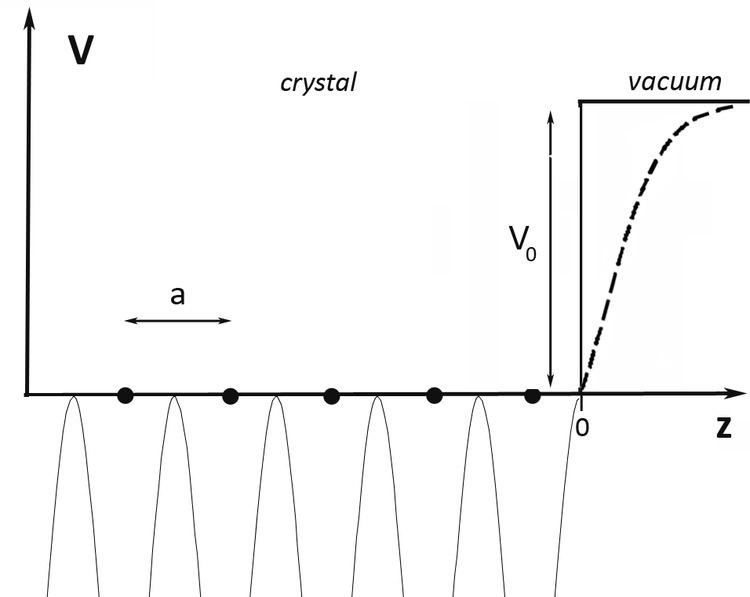
A simplified model of the crystal potential in one dimension can be sketched as shown in figure 1 . In the crystal, the potential has the periodicity, a, of the lattice while close to the surface it has to somehow attain the value of the vacuum level. The step potential (solid line) shown in figure 1 is an oversimplification which is mostly convenient for simple model calculations. At a real surface the potential is influenced by image charges and the formation of surface dipoles and it rather looks as indicated by the dashed line.
Given the potential in figure 1, it can be shown that the one-dimensional single-electron Schrödinger equation gives two qualitatively different types of solutions.
The first type of solution can be obtained for both metals and semiconductors. In semiconductors though, the associated eigenenergies have to belong to one of the allowed energy bands. The second type of solution exists in forbidden energy gap of semiconductors as well as in local gaps of the projected band structure of metals. It can be shown that the energies of these states all lie within the band gap. As a consequence, in the crystal these states are characterized by an imaginary wavenumber leading to an exponential decay into the bulk.
Shockley states and Tamm states
In the discussion of surface states, one generally distinguishes between Shockley states and Tamm states, named after the American physicist William Shockley and the Russian physicist Igor Tamm. However, there is no real physical distinction between the two terms, only the mathematical approach in describing surface states is different.
Topological surface states
All materials can be classified by a single number, a topological invariant; this is constructed out of the bulk electronic wave functions, which are integrated in over the Brillouin zone, in a similar way that the genus is calculated in geometric topology. In certain materials the topological invariant can be changed when certain bulk energy bands invert due to strong spin-orbital coupling. At the interface between an insulator with non-trivial topology, a so-called topological insulator, and one with a trivial topology, the interface must become metallic. More over, the surface state must have linear Dirac like dispersion with a crossing point which is protected by time reversal symmetry. Such a state is predicted to be robust under disorder, and therefore cannot be easily localized.
SEE http://rmp.aps.org/abstract/RMP/v82/i4/p3045_1
Surface states in metals
A simple model for the derivation of the basic properties of states at a metal surface is a semi-infinite periodic chain of identical atoms. In this model, the termination of the chain represents the surface, where the potential attains the value V0 of the vacuum in the form of a step function, figure 1. Within the crystal the potential is assumed periodic with the periodicity a of the lattice. The Shockley states are then found as solutions to the one-dimensional single electron Schrödinger equation
with the periodic potential
where l is an integer, and P is the normalization factor. The solution must be obtained independently for the two domains z<0 and z>0, where at the domain boundary (z=0) the usual conditions on continuity of the wave function and its derivatives are applied. Since the potential is periodic deep inside the crystal the electronic wave functions must be Bloch waves here. The solution in the crystal is then a linear combination of an incoming wave and a wave reflected from the surface. For z>0 the solution will be required to decrease exponentially into the vacuum
The wave function for a state at a metal surface is qualitatively shown in figure 2. It is an extended Bloch wave within the crystal with an exponentially decaying tail outside the surface. The consequence of the tail is a deficiency of negative charge density just inside the crystal and an increased negative charge density just outside the surface, leading to the formation of a dipole double layer. The dipole perturbs the potential at the surface leading, for example, to a change of the metal work function.
Surface states in semiconductors
The nearly free electron approximation can be used to derive the basic properties of surface states for narrow gap semiconductors. The semi-infinite linear chain model is also useful in this case. However, now the potential along the atomic chain is assumed to vary as a cosine function
whereas at the surface the potential is modeled as a step function of height V0. The solutions to the Schrödinger equation must be obtained separately for the two domains z < 0 and z > 0. In the sense of the nearly free electron approximation, the solutions obtained for z < 0 will have plane wave character for wave vectors away from the Brillouin zone boundary
Here
demonstrating the band splitting at the edges of the Brillouin zone, where the width of the forbidden gap is given by 2V. The electronic wave functions deep inside the crystal, attributed to the different bands are given by
Where C is a normalization constant. Near the surface at z = 0, the bulk solution has to be fitted to an exponentially decaying solution, which is compatible with the constant potential V0.
It can be shown that the matching conditions can be fulfilled for every possible energy eigenvalue which lies in the allowed band. As in the case for metals, this type of solution represents standing Bloch waves extending into the crystal which spill over into the vacuum at the surface. A qualitative plot of the wave function is shown in figure 2.
If imaginary values of κ are considered, i.e. κ = - i·q for z ≤ 0 and one defines
one obtains solutions with a decaying amplitude into the crystal
The energy eigenvalues are given by
E is real for large negative z, as required. Also in the range
Surface states of a three-dimensional crystal
The results for surface states of a monatomic linear chain can readily be generalized to the case of a three-dimensional crystal. Because of the two-dimensional periodicity of the surface lattice Bloch's theorem must hold for translations parallel to the surface. As a result, the surface states can be written as the product of a Bloch waves with k-values
The energy of this state is increased by a term
where m* is the effective mass of the electron. The matching conditions at the crystal surface, i.e. at z=0, have to be satisfied for each
True surface states and surface resonances
A surface state is described by the energy
Tamm states
Surface states that are calculated in the framework of a tight-binding model are often called Tamm states. In the tight binding approach, the electronic wave functions are usually expressed as a linear combinations of atomic orbitals (LCAO), see figure 5. In this picture, it is easy to comprehend that the existence of a surface will give rise to surface states with energies different from the energies of the bulk states: Since the atoms residing in the topmost surface layer are missing their bonding partners on one side their orbitals have less overlap with the orbitals of neighboring atoms. The splitting and shifting of energy levels of the atoms forming the crystal is therefore smaller at the surface than in the bulk.
If a particular orbital is responsible for the chemical bonding, e.g. the sp3 hybrid in Si or Ge, it is strongly affected by the presence of the surface, bonds are broken, and the remaining lobes of the orbital stick out from the surface. They are called dangling bonds. The energy levels of such states are expected to significantly shift from the bulk values.
In contrast to the nearly free electron model used to describe the Shockley states, the Tamm states are suitable to describe also transition metals and wide bandgap semiconductors.
Extrinsic surface states
Surface states originating from clean and well ordered surfaces are usually called intrinsic. These states include states originating from reconstructed surfaces, where the two-dimensional translational symmetry gives rise to the band structure in the k space of the surface.
Extrinsic surface states are usually defined as states not originating from a clean and well ordered surface. Surfaces that are fit into the category extrinsic are :
- Surfaces with defects, where the translational symmetry of the surface is broken.
- Surfaces with adsorbates
- Interfaces between two material such as a semiconductor-oxide or semiconductor-metal interfaces
- Interfaces between solid and liquid phases.
Generally, extrinsic surface states cannot easily be characterized in terms of their chemical, physical or structural properties.
Angle resolved photoemission spectroscopy (ARPES)
An experimental technique to measure the dispersion of surface states is angle resolved photoemission spectroscopy (ARPES) or angle resolved ultraviolet photoelectron spectroscopy (ARUPS).