
 | ||
A multigate device or multiple-gate field-effect transistor (MuGFET) refers to a MOSFET (metal–oxide–semiconductor field-effect transistor) that incorporates more than one gate into a single device. The multiple gates may be controlled by a single gate electrode, wherein the multiple gate surfaces act electrically as a single gate, or by independent gate electrodes. A multigate device employing independent gate electrodes is sometimes called a multiple-independent-gate field-effect transistor (MIGFET). Multigate transistors are one of the several strategies being developed by CMOS semiconductor manufacturers to create ever-smaller microprocessors and memory cells, colloquially referred to as extending Moore's law.
Contents
- Types
- Planar double gate transistor
- FlexFET
- FinFET
- Gate all around GAA FET
- Industry need
- Integration challenges
- Compact modeling
- References
Development efforts into multigate transistors have been reported by AMD, Hitachi, IBM, Infineon Technologies, Intel Corporation, TSMC, Freescale Semiconductor, University of California, Berkeley, and others, and the ITRS predicted correctly that such devices will be the cornerstone of sub-32 nm technologies. The primary roadblock to widespread implementation is manufacturability, as both planar and non-planar designs present significant challenges, especially with respect to lithography and patterning. Other complementary strategies for device scaling include channel strain engineering, silicon-on-insulator-based technologies, and high-k/metal gate materials.
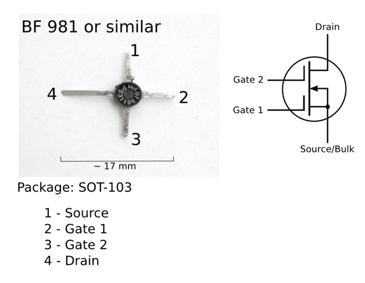
Dual-gate MOSFETs are commonly used in VHF mixers and in sensitive VHF front-end amplifiers. They are available from manufacturers such as Motorola, NXP, and Hitachi.
Types
Dozens of multigate transistor variants may be found in the literature. In general, these variants may be differentiated and classified in terms of architecture (planar vs. non-planar design) and number of channels/gates (2, 3, or 4).
Planar double-gate transistor
The first international demonstration of the multigate devices family using thin Silicon film was performed with a double-gate MOSFET []. The double-gate control of silicon-on-insulator (SOI) transistors was used to force the whole silicon film (interface layers and volume) in strong inversion (called “Volume-Inversion MOSFET”) or strong accumulation (called “Volume-Accumulation MOSFET”). This original method of transistor operation, at the origin of the unique electrostatic properties and scalability of multigate devices, offered excellent device performance, in particular great increases in subthreshold slope, transconductance, and drain current. A simulation program and experiments on SIMOX structures was used to study this new type of device.
Planar double-gate transistors employ conventional planar (layer by layer) manufacturing processes to create double-gate devices, avoiding more stringent lithography requirements associated with non-planar, vertical transistor structures. In planar double-gate transistors the drain–source channel is sandwiched between two independently fabricated gate/gate-oxide stacks. The primary challenge in fabricating such structures is achieving satisfactory self-alignment between the upper and lower gates.
FlexFET
FlexFET is a planar, independently double-gated transistor with a damascene metal top gate MOSFET and an implanted JFET bottom gate that are self-aligned in a gate trench. This device is highly scalable due to its sub-lithographic channel length; non-implanted ultra-shallow source and drain extensions; non-epi raised source and drain regions; and gate-last flow. FlexFET is a true double-gate transistor in that (1) both the top and bottom gates provide transistor operation, and (2) the operation of the gates is coupled such that the top gate operation affects the bottom gate operation and vice versa. Flexfet was developed and is manufactured by American Semiconductor, Inc.
FinFET
The term FinFET (fin field-effect transistor) was coined by University of California, Berkeley, researchers (Profs. Chenming Hu, Tsu-Jae King-Liu and Jeffrey Bokor) to describe a nonplanar, double-gate transistor built on an SOI substrate, based on the earlier DELTA (single-gate) transistor design. The distinguishing characteristic of the FinFET is that the conducting channel is wrapped by a thin silicon "fin", which forms the body of the device. The thickness of the fin (measured in the direction from source to drain) determines the effective channel length of the device. The wrap-around gate structure provides a better electrical control over the channel and thus helps in reducing the leakage current and overcoming other short-channel effects.
In current usage the term FinFET has a less precise definition. Among microprocessor manufacturers, AMD, IBM, and Freescale describe their double-gate development efforts as FinFET development, whereas Intel avoids using the term when describing their closely related tri-gate architecture (see #Tri-gate transistor). In the technical literature, FinFET is used somewhat generically to describe any fin-based, multigate transistor architecture regardless of number of gates.
A 25 nm transistor operating on just 0.7 volt was demonstrated in December 2002 by TSMC (Taiwan Semiconductor Manufacturing Company). The "Omega FinFET" design is named after the similarity between the Greek letter omega (Ω) and the shape in which the gate wraps around the source/drain structure. It has a gate delay of just 0.39 picosecond (ps) for the N-type transistor and 0.88 ps for the P-type.
FinFET can also have two electrically independent gates, which gives circuit designers more flexibility to design with efficient, low-power gates.
In 2012, Intel started using FinFETs for its future commercial devices. Leaks suggest that Intel's FinFET has an unusual shape of a triangle rather than rectangle, and it is speculated that this might be either because a triangle has a higher structural strength and can be more reliably manufactured or because a triangular prism has a higher area-to-volume ratio than a rectangular prism, thus increasing switching performance.
In September 2012, GlobalFoundries announced plans to offer a 14-nanometer process technology featuring FinFET three-dimensional transistors in 2014. The next month, the rival company TSMC announced start early or "risk" production of 16 nm FinFETS in November 2013.
In March 2014, TSMC announced that it is nearing implementation of several 16 nm FinFETs die-on wafers manufacturing processes:
AMD announced a 14 nm FinFET GPU based on their Polaris chip architecture in January 2016. The company expects the design to provide a "generational jump in power efficiency" while also offering stable frame rates for graphics, gaming, virtual reality, and multimedia applications.
Tri-gate or 3D transistor (not to be confused with 3D microchips) fabrication is used by Intel Corporation for the nonplanar transistor architecture used in Ivy Bridge, Haswell and Skylake processors. These transistors employ a single gate stacked on top of two vertical gates, allowing essentially three times the surface area for electrons to travel. Intel reports that their tri-gate transistors reduce leakage and consume far less power than current transistors. This allows up to 37% higher speed or a power consumption at under 50% of the previous type of transistors used by Intel.
Intel explains: "The additional control enables as much transistor current flowing as possible when the transistor is in the 'on' state (for performance), and as close to zero as possible when it is in the 'off' state (to minimize power), and enables the transistor to switch very quickly between the two states (again, for performance)." Intel has stated that all products after Sandy Bridge will be based upon this design.
Intel was the first company to announce this technology. In September 2002, Intel announced their creation of "triple-gate transistors" to maximize "transistor switching performance and decreases power-wasting leakage". A year later, in September 2003, AMD announced that it was working on similar technology at the International Conference on Solid State Devices and Materials. No further announcements of this technology were made until Intel's announcement in May 2011, although it was stated at IDF 2011, that they demonstrated a working SRAM chip based on this technology at IDF 2009.
On April 23, 2012 Intel released a new line of CPUs, termed Ivy Bridge, which feature tri-gate transistors. Intel has been working on its tri-gate architecture since 2002, but it took until 2011 to work out mass-production issues. The new style of transistor was described on May 4, 2011, in San Francisco. Intel factories are expected to make upgrades over 2011 and 2012 to be able to manufacture the Ivy Bridge CPUs. As well as being used in Intel's Ivy Bridge chips for desktop PCs, the new transistors will also be used in Intel's Atom chips for low-powered devices.
The term tri-gate is sometimes used generically to denote any multigate FET with three effective gates or channels.
Gate-all-around (GAA) FET
Gate-all-around FETs are similar in concept to FinFETs except that the gate material surrounds the channel region on all sides. Depending on design, gate-all-around FETs can have two or four effective gates. Gate-all-around FETs have been successfully characterized both theoretically and experimentally. They have also been successfully etched onto InGaAs nanowires, which have a higher electron mobility than silicon.
Industry need
Planar transistors have been the core of integrated circuits for several decades, during which the size of the individual transistors has steadily decreased. As the size decreases, planar transistors increasingly suffer from the undesirable short-channel effect, especially "off-state" leakage current, which increases the idle power required by the device.
In a multigate device, the channel is surrounded by several gates on multiple surfaces. It thus provides a better electrical control over the channel, allowing more effective suppression of "off-state" leakage current. Multiple gates also allow enhanced current in the "on" state, also known as drive current. Multigate transistors also provide a better analog performance due to a higher intrinsic gain and lower channel length modulation. These advantages translate to lower power consumption and enhanced device performance. Nonplanar devices are also more compact than conventional planar transistors, enabling higher transistor density which translates to smaller overall microelectronics.
Integration challenges
The primary challenges to integrating nonplanar multigate devices into conventional semiconductor manufacturing processes include:
Compact modeling
BSIMCMG106.0.0, officially released on March 1, 2012 by UC Berkeley BSIM Group, is the first standard model for FinFETs. BSIM-CMG is implemented in Verilog-A. Physical surface-potential-based formulations are derived for both intrinsic and extrinsic models with finite body doping. The surface potentials at the source and drain ends are solved analytically with poly-depletion and quantum mechanical effects. The effect of finite body doping is captured through a perturbation approach. The analytic surface potential solution agrees closely with the 2-D device simulation results. If the channel doping concentration is low enough to be neglected, computational efficiency can be further improved by a setting a specific flag (COREMOD = 1).
All of the important multi-gate (MG) transistor behavior is captured by this model. Volume inversion is included in the solution of Poisson’s equation, hence the subsequent I–V formulation automatically captures the volume-inversion effect. Analysis of electrostatic potential in the body of MG MOSFETs provided a model equation for short-channel effects (SCE). The extra electrostatic control from the end gates (top/bottom gates) (triple or quadruple-gate) is also captured in the short-channel model.