
Max. CPU clock rate 1.60 GHz to 3.60 GHz L1 cache 64 KB per core | Product code 80623 (desktop) L2 cache 256 KB per core | |
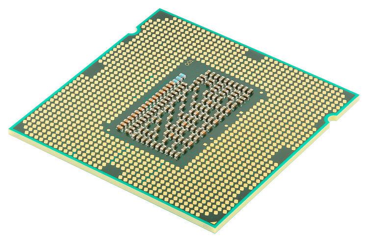 | ||
L3 cache 1 MB to 8 MB shared10 MB to 15 MB (Extreme)3 MB to 20 MB (Xeon) Model Celeron SeriesPentium SeriesCore i3/i5/i7/i7 Extreme SeriesXeon E3/E5 Series | ||
Sandy Bridge is the codename for a microarchitecture developed by Intel beginning in 2005 for central processing units in computers to replace the Nehalem microarchitecture. Intel demonstrated a Sandy Bridge processor in 2009, and released first products based on the architecture in January 2011 under the Core brand. Developed primarily by the Israeli branch of Intel, the codename was originally "Gesher" (meaning "bridge" in Hebrew).
Contents
- Technology
- Models and steppings
- Performance
- List of Sandy Bridge processors
- Mobile platform
- Cougar Point chipset flaw
- Overclocking
- Chipset
- vPro remote control
- Intel Insider
- Software development kit
- Roadmap
- References
Sandy Bridge implementations targeted a 32 nanometer manufacturing process, while Intel's subsequent product, codenamed Ivy Bridge, uses a 22 nanometer process. The Ivy Bridge die shrink, known in the Intel Tick-Tock model as the "tick", is based on FinFET (non-planar, "3D") tri-gate transistors. Intel demonstrated the Ivy Bridge processors in 2011.
A Core i7 2600 Sandy Bridge CPU at 3.4 GHz with 1333MHz DDR3 memory reaches 83 GFLOPS performance in the Whetstone benchmark and 118,000 MIPS in the Dhrystone benchmark.
Technology
Developed primarily by the Israel branch of Intel, the codename was originally "Gesher" (meaning "bridge" in Hebrew). The name was changed to avoid being associated with the defunct Gesher political party; the decision was led by Ron Friedman, vice president of Intel managing the group at the time. Intel demonstrated a Sandy Bridge processor with A1 stepping at 2 GHz during the Intel Developer Forum in September 2009.
Upgraded features from Nehalem include:
Models and steppings
All Sandy Bridge processors with one, two, or four cores report the same CPUID model 0206A7h and are closely related. The stepping number can not be seen from the CPUID but only from the PCI configuration space. The later Sandy Bridge-E processors with up to eight cores and no graphics are using CPUIDs 0206D6h and 0206D7h. Ivy Bridge CPUs all have CPUID 0306A9h to date, and are built in four different configurations differing in the number of cores, L3 cache and GPU execution units.
Performance
List of Sandy Bridge processors
1Processors featuring Intel's HD 3000 graphics are set in bold. Other processors feature HD 2000 graphics, HD Graphics (Pentium and Celeron models) or no graphics core (Graphics Clock rate indicated by N/A).
Suffixes to denote:
NOTE: 3970X, 3960X, 3930K, and 3820 are actually of Sandy Bridge-E edition.
Mobile platform
Suffixes to denote:
Cougar Point chipset flaw
On 31 January 2011, Intel issued a recall on all 67-series motherboards due to a flaw in the Cougar Point Chipset. A hardware problem, in which the chipset's SATA II ports may fail over time, cause failure of connection to SATA devices, though data is not at risk. Intel claims that this problem will affect only 5% of users over 3 years, however, heavier I/O workloads can exacerbate the problem.
Intel stopped production of flawed B2 stepping chipsets and began producing B3 stepping chipsets with the silicon fix. Shipping of these new chipsets started on 14 February 2011 and Intel estimated full recovery volume in April 2011. Motherboard manufacturers (such as ASUS and Gigabyte Technology) and computer manufacturers (such as Dell and Hewlett-Packard) stopped selling products that involved the flawed chipset and offered support for affected customers. Options ranged from swapping for B3 motherboards to product refunds.
Sandy Bridge processor sales were temporarily on hold, as one cannot use the CPU without a motherboard. However, processor release dates were not affected. After two weeks, Intel continued shipping some chipsets, but manufacturers had to agree to a set of terms that will prevent customers from encountering the bug.
Overclocking
With Sandy Bridge, Intel has tied the speed of every bus (USB, SATA, PCI, PCI-E, CPU cores, Uncore, memory etc.) to a single internal clock generator issuing the basic 100 MHz Base Clock (BClk). With CPUs being multiplier locked, the only way to overclock is to increase the BClk, which can be raised by only 5–7% without other hardware components failing. As a work around, Intel made available K/X-series processors, which feature unlocked multipliers; with a multiplier cap of 57 for Sandy Bridge. For the Sandy Bridge E platform, there is alternative method known as the BClk ratio overclock.
During IDF (Intel Developer Forum) 2010, Intel demonstrated an unknown Sandy Bridge CPU running stably overclocked at 4.9 GHz on air cooling.
Chipset
Non-K edition CPUs can overclock up to four bins from its turbo multiplier. Refer here for chipset support.
vPro remote-control
Sandy and Ivy Bridge processors with vPro capability have security features that can remotely disable a PC or erase information from hard drives. This can be useful in the case of a lost or stolen PC. The commands can be received through 3G signals, Ethernet, or Internet connections. AES encryption acceleration will be available, which can be useful for video conferencing and VoIP applications.
Intel Insider
Sandy and Ivy Bridge processors contain a DRM technology that some video streaming web sites rely on to restrict use of their content. Such web sites offer 1080p streaming to users with such CPUs and downgrade the quality for other users.
Software development kit
With the introduction of the Sandy Bridge microarchitecture, Intel also introduced the Intel Data Plane Development Kit (Intel DPDK) to help developers of communications applications take advantage of the platform in packet processing applications, and network processors.
Roadmap
Intel demonstrated the Haswell architecture in September 2011, released in 2013 as the successor to Sandy Bridge and Ivy Bridge.