
Molar mass 351.14 g/mol Appearance black/lead-gray solid | Density 7.78 g/cm³ | |
 | ||
Molybdenum(IV) telluride, molybdenum ditelluride or just molybdenum telluride is a compound of molybdenum and tellurium with formula MoTe2, corresponding to a mass percentage of 27.32% molybdenum and 72.68% tellurium. It can crystallise in two dimensional sheets which can be thinned down to monolayers that are flexible and almost transparent. It is a semiconductor, and can fluoresce. It is part of a class of materials called transition metal dichalcogenides. As a semiconductor the band gap lies in the infrared region. This raises the potential use as a semiconductor in electronics or an infrared detector.
Contents
Preparation
MoTe2 can be prepared by heating the correct ratio of the elements together at 1100 °C in a vacuum. Another method is via vapour deposition, where molybdenum and tellurium are volatilised in bromine gas and then deposited. Using bromine results in forming an n-type semiconductor, whereas using tellurium only results in a p-type semiconductor.
The amount of tellurium in molybdenum ditelluride can vary, with tellurium being slightly deficient unless it is added in excess during production. Tellurium molecular proportion range from 1.97 to 2. Excess tellurium deposited during this process can be dissolved off with sulfuric acid.
By annealing molybdenum film in a tellurium vapour at 850 to 870 °C for several hours, a thin layer of MoTe2 is formed.
An amorphous form can be produced by sonochemically reacting molybdenum hexacarbonyl with tellurium dissolved in decalin.
Molybdenum ditelluride can be formed by electrodeposition from a solution of molybdic acid (H2MoO4) and tellurium dioxide (TeO2). The product can be electroplated on stainless steel or indium tin oxide.
Colour
In powdered form MoTe2 is black.
Very thin crystals of MoTe2 can be made using sticky tape. When they are thin around 500 nm thick red light can be transmitted. Even thinner layers can be orange or transparent. An absorption edge occurs in the spectrum with wavelengths longer than 6720 Å transmitted and shorter wavelengths heavily attenuated. At 77 K this edge changes to 6465 Å. This corresponds to deep red.
Infrared
MoTe2 reflects about 43% in the infrared band but has a peak at 234.5 cm−1 and a minimum at 245.8 cm−1.
As the temperature is lowered the absorption bands become narrower. At 77 K there are absorption peaks at 1.141, 1.230, 1.489, 1.758, 1.783, 2.049, 2.523, 2.578, and 2.805 eV.
Exciton energy levels are at 1.10 eV, called A, and 1.48 eV, called B, with a difference of 0.38 eV.
Raman spectrum
The Raman spectrum has four lines with wavenumbers of 25.4, 116.8, 171.4, and a double one at 232.4 and 234.5 cm−1. The peak at 234.5 cm−1 is due to E12g mode, especially in nanolayers, but the thicker forms and the bulk has the second peak at 232.4 cm−1 also perhaps due to the E21u phonon mode. The peak near 171.4 cm−1 comes from the A1g. 138 and 185 cm−1 peaks may be due to harmonics. B12g is assigned to a peak around 291 cm−1 in nanolayers with few layers. The E12g frequency increases as the number of layers decreases to 236.6 cm−1 for single layer. The A1g mode lowers its frequency as the number of layers decreases, becoming 172.4 cm−1 for the monolayer.
Crystal form
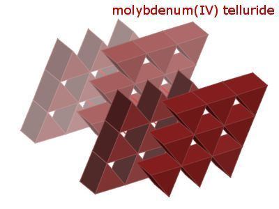
At room temperature MoTe2 crystallises in the hexagonal system similar to molybdenum disulfide. Crystals are platy or flat. MoTe2 has unit cell sizes of a=3.519 Å c=13.964 Å and a specific gravity of 7.78 gcm−3. Each molybdenum atom is surrounded by six tellurium atoms in a trigonal prism with the separation of these Mo and Te atoms being 2.73 Å. This results in sublayers of molybdenum sandwiched between two sublayers of tellurium atoms, and then this three layer structure is stacked. Each layer is 6.97 Å thick. Within this layer two tellurium atoms in the same sublayer subtend an angle of 80.7°. The tellurium atoms on one sublayer are directly above those in the lower sublayer, and they subtend an angle of 83.1° at the Molybdenum atom. The other Te-Mo-Te angle across sublayers is 136.0°. The distance between molybdenum atoms within a sublayer is 3.518 Å. This is the same as the distance between tellurium atoms in a sublayer. The distance between a tellurium atom in one sublayer and the atom in the other sublayer is 3.60 Å.
The layers are only bonded together with van der Waals force. The distance between tellurium atoms across the layers is 3.95 Å. The tellurium atom at the bottom of one layer is aligned with the centre of a triangle of tellurium atoms on the top of the layer below. The layers are thus in two different positions. The crystal is very easily cleaved on the plane between the three layer sheets. The sizes change with temperature, at 100 K a=3.492 Å and at 400 K is 3.53 Å. In the same range c changes from 13.67 Å to 14.32 Å due to thermal expansion. The hexagonal form is also called 2H-MoTe2, where "H" stands for hexagonal, and "2" means that the layers are in two different positions. Every second layer is positioned the same.
At temperatures above 900 °C MoTe2 crystallises in a monoclinic form, with space group P21/m with unit cell sizes of a=6.33 Å b=3.469 Å and c=13.86 Å with the angle β=93°55′. The high temperature form has rod shaped crystals. The measured density of this polymorph is 7.5 gcm−3, but in theory it should be 7.67 gcm−3. Tellurium atoms form a distorted octahedron around the molybdenum atoms. This high temperature form, termed β–MoTe2 can be quenched to room temperature by rapid cooling. In this metastable state β-MoTe2 can survive below 500 °C. When metastable β–MoTe2 is cooled below −20 °C, its crystal form changes to orthorhombic. This is because the monoclinic angle c changes to 90°. This form is called β'–MoTe2.
The transition from α- to β-MoTe2 happens at 820 °C, but if Te is reduced by 5% the required transition temperature increases to 880 °C. K. Ueno and K. Fukushima claim that when the α form is heated in a low or high vacuum that it oxidises to from MoO2 and that reversible phase transitions do not take place.
In bulk, MoTe2 can be produced as a single crystal with difficulty, but can also be made as a powder, as a polycrystalline form, as a thin film, as a nanolayer consisting of a few TeMoTe sheets, a bilayer consisting of two sheets or as a monolayer with one sheet.
Thin nanolayer forms of α-MoTe2 have different symmetry depending on how many layers there are. With an odd number of layers the symmetry group is D13h without inversion, but for an even number of layers, the lattice is the same if inverted and the symmetry group is D33d. Nanotubes with a 20–60 nm diameter can be made by heat treating amorphous MoTe2.
Fluorescence
The fundamental properties of MoTe2 and its interaction with the environment have been established by B. Chen et al. from Arizona State University.
Electrical
N-type bulk α-MoTe2 has an electrical conductivity of 8.3 Ω−1cm−1 with 5×10¹⁷ mobile electrons per cubic centimeter. P-type bulk MoTe2 has an electrical conductivity of 0.2 Ω−1cm−1 and a hole concentration of 3.2×1016 cm−3. The peak electrical conductivity is around 235K, dropping off slowly with decreasing temperatures, but also reducing to a minimum around 705K. Above 705K conductivity increases again with temperature. Powdered MoTe2 has a much higher resistance.
β–MoTe2 has a much lower resistance than α–MoTe2 by more than a thousand times with values around 0.002 Ωcm. It is much more metallic in nature. In the β form the molybdenum atoms are closer together so that the conduction band overlaps. At room temperature resistance is 0.000328 Ωcm.
Td-MoTe2 (orthorhombic β form) has a resistance about 10% lower than the β form, and the resistance shows hysteresis of several degrees across the transition point around 250K. The resistance drops roughly linearly with decreasing temperature. At 180K resistance is 2.52×10⁻⁴ Ωcm. Below 30K the resistance drops quadratically with temperature, approaching no resistance as absolute zero is approached.
At low electric current levels the voltage is proportional to the current in the α form. With high electric currents MoTe2 shows negative resistance, where as the current increases the voltage across the material decreases. This means there is a maximum voltage that can be applied. In the negative resistance region the current must be limited, otherwise thermal runaway will destroy the item made from the material.
The Hall constant at room temperature is around 120 cm3/Coulomb for stochiometric α-MoTe2. But as Te is depleted the constant drops to close to 0 for compositions in the range MoTe1.94 to MoTe1.95.
The Seebeck coefficient is about 450 μV/K at room temperature for pure MoTe2, but this drops to 0 for MoTe1.95. The Seebeck coefficient increases as temperature drops.
Semiconductor
In the bulk α form of MoTe2 the material is a semiconductor with a room temperature indirect band gap of 0.88 eV and a direct band gap of 1.02 eV. If instead of bulk forms, nanolayers are measured, the indirect band gap increases as the number of layers is reduced. α-MoTe2 changes from an indirect to a direct band gap material in very thin slices. It is a direct bandgap material when it is one or two layers (monolayer or bilayer).
The band gap is reduced for tellurium deficient MoTe2. It can be reduced from 0.97 to 0.5.
The work function is 4.1 eV.
Magnetism
α–MoTe2 is diamagnetic whereas β–MoTe2 is paramagnetic.
X-ray
X-ray photoelectron spectroscopy on clean MoTe2 crystal surfaces show peaks at 231 and 227.8 eV due to molybdenum 3d3/2 and 3d5/2; with 582.9 and 572.5 due to tellurium 3d3/2 and 3d5/2 electrons.
The X-ray K absorption edge occurs at 618.41±0.04 X units compared to molybdenum metal at 618.46 xu.
Microscopy
Atomic force microscopy (AFM) of the van der Waals surface of α-MoTe2 shows alternating rows of smooth balls, which are the tellurium atoms. AFM images are often done on a silica (SiO2) surface on silicon. A monolayer of α-MoTe2 has its surface 0.9 nm above the silica, and each extra layer of α-MoTe2 adds 0.7 nm.
Scanning tunneling microscopy (STM) of α-MoTe2 reveals a hexagonal grid like chicken wire, where the molybdenum atoms are contributing to the current. Higher bias voltages are required to get an image, either over 0.5 V or below −0.3 V.
β-MoTe2 surfaces examined with scanning tunneling microscopy can show either a pattern of tellurium atoms or a pattern of molybdenum atoms on different parts. When the scanning tip is further from the surface only tellurium atoms are visible. This is explained by the dz2 orbitals from molybdenum penetrating up through the surface layer of tellurium. The molybdenum can supply a much bigger current than tellurium. But at greater distance only the p orbital from tellurium can be detected. Lower voltages than used for α form still produce atomic images.
Friction force microscopy (FFM) has been used to get a slip-stick image at a resolution below that of the unit cell.
Thermal
Heat in α-MoTe2 is due to vibrations of the atoms. These vibrations can be resolved into phonons in which the atoms move backwards and forwards in different ways. For a monolayer twisting of the tellurium atoms within the plane is termed E″, a scissoring action where tellurium moves in the plane of the layer is termed E′. Where tellurium vibrates in opposite directions perpendicular to the layer out of the plane the phonon mode is A′1 and where the tellurium moves in the same direction opposite to the molybdenum the mode is called A″1. Of these modes the first three are active in the Raman spectrum. In a bilayer there is an extra interaction between the atoms on the bottom of one layer and the atom on the top of the under layer. The mode symbols are modified with a suffix, "g" or "u" . In the bulk form with many layers, the modes are called A1g (corresponding to A′1 in the monolayer), A2u, B1u B2g, E1g, E1u, E2g and E2u. Modes E1g, E12g, E22g, and A1g are Raman active. Modes E11u, E21u, A12u, and A22u are infrared active.
Molar heat of formation of α-MoTe2 is −6 kJ/mol from β-MoTe2. Heat of formation of β-MoTe2 is −84 kJ/mol. For Mo3Te4 it is −185 kJ/mol.
Thermal conductivity is 2 Wm−1K−1.
Pressure
Under pressure α-MoTe2 is predicted to become a semimetal between 13 and 19 GPa. The crystal form should stay the same at pressures up to 100 GPa. β-MoTe2 is not predicted to become more metallic under pressure.
Other
Poisson ratio V∞=0.37. Monolayer relaxed ion elastic coefficients C11=80 and C12=21. Monolayer relaxed ion piezoelectric coefficient d11=9.13.
Reactions
MoTe2 gradually oxidises in air forming molybdenum dioxide (MoO2). At elevated temperatures MoTe2 oxidation produces Te2MoO7 and TeMo5O16. Other oxidation products include molybdenum trioxide, tellurium, and tellurium dioxide. Flakes of molybdenum ditelluride that contain many defects have lower luminescence, and absorb oxygen from the air, losing their luminescence.
When heated to high temperatures, tellurium evaporates from molybdenum ditelluride, producing the tellurium deficient forms and then Mo2Te3. This change is disruptive to experiments as the properties change significantly with Te content as well as with temperature. The vapour pressure of Te2 over hot MoTe2 is given by 108.398-11790/T. On further heating Mo2Te3 gives off Te2 vapour. The partial pressure of Te2 is given by 105.56-9879/T where T is in K and the pressure is in bars. Molybdenum metal is left behind.
The surface on the flat part of the hexagonal crystal (0001) is covered in tellurium, and is relatively inert. It can have other similar layers added onto it. Tungsten disulfide and tungsten diselenide layers have been added to molybdenum ditelluride by van der Waals epitaxy (vdWE). Gold can be deposited on the cleavage surfaces of MoTe2. On the α form gold tends to be isotropically deposited, but on the β form it makes elongated strips along the [010] crystal direction. Other substances that have been deposited on the crystal surface include indium selenide (InSe), cadmium sulfide (CdS), cadmium telluride (CdTe), tin disulfide (SnS2), tin diselenide (SnSe2), and tantalum diselenide (TaSe2). Some other monolayers are also predicted to be able to form on MoTe2 surfaces, including silicene. Silicene is claimed to become a zero-gap semiconductor on a bulk crystal, but have a metallic form on or between monolayers of MoTe2. Organic molecules can be incorporated as a layer on the van der Waals surface, including perylene tetracarboxylic acid anhydride.
The sheets in α-MoTe2 can be separated and dispersed in water with a sodium cholate surfactant and sonication. It forms an olive green suspension. MoTe2 is hydrophobic, but the surfactant coats the surface with its lipophilic tail.
The sheets in α-MoTe2 are able to be penetrated by alkali metals such as lithium to form intercalation compounds. This property means that it could be used as an electrode in a lithium battery. Up to Li1.6MoTe2 can be formed. This material has a similar X-ray diffraction pattern to α-MoTe2.
André Morette, the first to make tellurides of molybdenum, discovered that it would burn in a flame, colouring it blue, and making a white smoke of tellurium dioxide. Dilute nitric acid can dissolve it by oxidation. However hot or cold hydrochloric or sulfuric acid could not attack MoTe2. However concentrated sulfuric acid at 261 °C does completely dissolve MoTe2. Sodium hydroxide solution partially dissolves MoTe2.
Related substances
Another molybdenum telluride has formula Mo2Te3.
Yet another molybdenum telluride, called hexamolybdenum octatelluride Mo6Te8 forms black crystals shaped like cubes. It is formed when the elements in the correct ratio are heated together at 1000 °C for a week. It is related to the Chevrel phases, but without an extra metallic cation, however it is not superconducting.
Metal atoms and organic molecules can be intercalated between the layers of MoTe2.
Uses
Potential uses for MoTe2 are for lubricant, electronics, optoelectronics or a photoelectric cell material. Diodes have been fabricated from MoTe2 by baking a p-type material in bromine. The diode's current versus voltage plot shows very little current with reverse bias, an exponential region with dV/dln(j) of 1.6, and at higher voltages (>0.3V) a linear response due to resistance. When operated as a capacitor, the capacitance varies as the inverse square of the bias, and also drops for higher frequencies. Transistors have also been built from MoTe2. MoTe2 has potential to build low power electronics. Field effect transistors (FET) have been built from a bilayer, trilayer and thicker nanolayers. An ambipolar FET has been built, and also a FET that can operate in n- or p-modes which had two top electrodes.
Because MoTe2 has two phases, devices can be constructed that mix the 2H semiconductor, and the 1T metallic form. A laser can rapidly heat a thin layer to transform it to the metallic form.
A FET can be constructed with a thin layer of molybdenum ditelluride covered with a liquid gate composed of an ionic liquid or an electrolyte such as potassium perchlorate dissolved in polyethylene glycol. With low gate voltages below 2 volts, the device operates in an electrostatic mode, where the current from drain to source is proportional to the gate voltage. Above 2 volts the device enters an intermediate region where current does not increase. Above 3.5 volts current leaks through the gate, and electrolysis occurs intercalating potassium atoms in the MoTe2 layer. The potassium intercalated molybdenum ditelluride becomes superconducting below 2.8 K.
As a lubricant molybdenum ditelluride can function well in a vacuum and at temperatures up to 500 °C with a coefficient of friction below 0.1. However molybdenum disulfide has a lower friction, and molybdenum diselenide can function at higher temperatures.
Related dichalcogenides can be fabricated into fairly efficient photoelectric cells.
Potentially, stacked monolayers of indium nitride and molybdenum ditelluride can result in improved properties for photovoltaics, including lower refractive index, and greater absorbance.
Cadmium telluride solar cells are often deposited on a backplate of molybdenum. Molybdenum ditelluride can form at the contact, and if this is n-type it will degrade the performance of the solar cell.
Small pieces of nanolayers of molybdenum ditelluride can be mixed in and dispersed in molten pewter without reacting, and it causes a doubling of the stiffness of the resultant composite.
Molybdenum ditelluride has been used as a substrate for examining proteins with an atomic force microscope. It is superior because the protein sticks harder than with more traditional materials such as mica.