
 | ||
Transition metal dichalcogenide (TMDC) monolayers are atomically thin semiconductors of the type MX2, with M a transition metal atom (Mo, W, etc.) and X a chalcogen atom (S, Se, or Te). One layer of M atoms is sandwiched between two layers of X atoms. They are part of the large and new family of the so-called 2D materials, name used to emphasize their extraordinary thinness. For example a MoS2 monolayer is only 6.5 Å thick.
Contents
- Crystal structure
- Transport properties
- Optical properties
- Mechanical properties
- Exfoliation
- Chemical vapor deposition
- Molecular beam epitaxy
- Band gap
- Spin orbit coupling
- Spin valley coupling and the electron valley degree of freedom
- Emission and absorption of light excitons
- References
The discovery of graphene shows how new physical properties emerge when a bulk crystal of macroscopic dimensions is thinned down to one atomic layer. Like graphite, TMDC bulk crystals are formed of monolayers bound to each other by Van-der-Waals attraction. TMDC monolayers have properties that are distinctly different from those of the semimetal graphene:
The work on TMDC monolayers is an emerging research and development field since the discovery of the direct bandgap and the potential applications in electronics and valley physics. TMDCs are often combined with other 2D materials like graphene and hexagonal boron nitride to make van der Waals heterostructure. These heterostructures need to be optimized to be possibly used as building blocks for a plenty of different devices such as transistors, solar cells, LEDs, photodetectors, fuel cells, photocatalytic and sensing devices. Some of these devices are already used in everyday life and can become smaller, cheaper and more efficient by using TMDC monolayers. Others are still being developed and promise to have a huge impact on our technology.
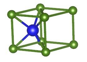
Crystal structure
In the macroscopic bulk crystal, or more precisely, for an even number of monolayers, the crystal structure has an inversion center. In the case of a monolayer (or any odd number of layers), the crystal has no inversion center. Two important consequences of that are:
These properties indicate that TMDC monolayers represent a promising platform to explore spin and valley physics with the corresponding possible applications.
Transport properties
At submicron scales, 3D materials no longer have the same behavior as their 2D form, which can be an advantage. For example, graphene has a very high carrier mobility, and accompanying lower losses through the Joule effect. But graphene has zero bandgap, which results in a disqualifying low on/off ratio in transistor applications. TMDC monolayers might be an alternative: they are structurally stable, display a band gap and show electron mobilities comparable to those of silicon, so they can be used to fabricate transistors.
In 2004, the first field-effect transistor (FET) made of bulk WSe2 was reported. It showed a mobility below 500 cm2 V−1 s−1 for p-type conductivity at room temperature, about half that of a silicon FET but a low on/off current ratio because the device was realised on the surface of a bulk crystal. FETs made of monolayer MoS2 showed an excellent on/off ratio exceeding 108.
High carrier mobility, high on/off ratio and small thickness (one monolayer) of TMDC devices are potentially interesting for such applications.
Optical properties
A semiconductor can absorb photons with energy larger than or equal to its bandgap. This means that light with a shorter wavelength is absorbed. Semiconductors are typically efficient emitters if the minimum of the conduction band energy is at the same position in k-space as the maximum of the valence band, i.e., the band gap is direct. The band gap of bulk TMDC material down to a thickness of two monolayers is still indirect, so the emission efficiency is lower compared to monolayered materials. The emission efficiency is about 104 greater for TMDC monolayer than for bulk material. The band gaps of TMDC monolayers are in the visible range (between 400 nm and 700 nm). The direct emission shows two transitions called A and B, separated by the spin-orbit coupling energy. The lowest energy and therefore most important in intensity is the A emission. Owing to their direct band gap, TMDC monolayers are promising materials for optoelectronics applications.
Atomic layers of MoS2 have been used as a phototransistor and ultrasensitive detectors. Phototransistors are important devices: the first with a MoS2 monolayer active region shows a photoresponsivity of 7.5 mA W−1 which is similar to graphene devices that reach 6.1 mA W−1. Multilayer MoS2 show higher photoresponsivities, about 100 mA W−1, which is similar to silicon devices. Making a gold contact at the far edges of a monolayer allows an ultrasensitive detector to be fabricated. Such a detector has a photoresponsivity reaching 880 A W−1, 106 greater than the first graphene photodetectors. This high degree of electrostatic control is due to the thin active region of the monolayer. Its simplicity and the fact that it has only one semiconductor region, whereas the current generation of photodetectors is typically a p-n junction, makes possible industrial applications such as high-sensitivity and flexible photodetectors. The only limitation for currently available devices is the slow photoresponse dynamics.
Mechanical properties
A monolayer of MoS2 can be strained at least up to 10%, comparable to graphene. Under the application of strain, a decrease in the direct and indirect band gap is measured that is approximately linear with strain. Importantly, the indirect bandgap decreases faster with applied strain to the monolayer than the direct bandgap, resulting in a crossover from direct to indirect band gap at a strain level of around 1%. As a result, the emission efficiency of monolayers is expected to decrease for highly strained samples. This property allows mechanical tuning of the electronic structure and also the possibility of fabrication of flexible electronics i.e. on flexible substrates.
Exfoliation
Exfoliation is a top down approach. In the bulk form, TMDCs are crystals made of layers, which are coupled by Van-der-Waals forces. These interactions are weaker than the chemical bonds between the Mo and S in MoS2, for example. So TMDC monolayers can be produced by micromechanical cleavage, just as graphene.
The crystal of TMDC is rubbed against the surface of another material (any solid surface). In practice, adhesive tape is placed on the TMDC bulk material and subsequently removed. The adhesive tape, with tiny TMDC flakes coming off the bulk material, is brought down onto a substrate. On removing the adhesive tape from the substrate, TMDC monolayer and multilayer flakes are deposited. This technique produces small samples of monolayer material, typically about 5–10 micrometers in diameter.
Large quantities of exfoliated material can also be produced using liquid-phase exfoliation by blending TMDC materials with solvents and polymers.
Chemical vapor deposition
Chemical vapor deposition is a bottom-up approach. For example, the synthesis of MoS2 is made using: SiO2 as a substrate, MoO3 and S powders used as reactants. The reactants are delivered on the substrate and the whole is heated to 650 Celsius degrees in the presence of N2. The size of the sample is larger than obtained with the exfolation technique.
Molecular beam epitaxy
Molecular beam epitaxy (MBE) is an established technique for growing semiconductor devices with atomic monolayer thickness control. As a promising demonstration, high-quality monolayer MoSe2 samples have been grown on graphene by MBE.
Band gap
In the bulk form, TMDC have an indirect gap in the center of the Brillouin zone, whereas in monolayer form the gap becomes direct and is located in the K points.
Spin-orbit coupling
For TMDCs, the atoms are heavy and the outer layers electronic states are from d-orbitals that have a strong spin-orbit coupling. This spin orbit coupling removes the spins degeneracy in both the conduction and valence band i.e. introduces a strong energy splitting between spin up and down states. In the case of MoS2, the spin splitting in conduction band is in the meV range, it is expected to be more pronounced in other material like WS2. The spin orbit splitting in the valence band is several hundred meV.
Spin-valley coupling and the electron valley degree of freedom
By controlling the charge or spin degree of freedom of carriers, as proposed by spintronics, novel devices have already been made. If there are different conduction/valence band extrema in the electronic band structure in k-space, the carrier can be confined in one of these valleys. This degree of freedom opens up a new field of physics: the controlling of carriers k-valley index, also called valleytronics.
For TMDC monolayers crystals, the parity symmetry is broken, there is no more inversion center. K valleys of different directions in the 2D hexagonal Brillouin zone are no longer equivalent. So there are two kinds of K valley called K+ and K-. Also there is a strong energy degeneracy of different spin states in valence band. The transformation of one valley to another is described by the time reversal operator. Moreover, crystal symmetry leads to valley dependent optical selection rules: a right circular polarized photon (σ+) initializes a carrier in the K+ valley and a left circular polarized photon (σ-) initializes a carrier in the K- valley. Thanks to these two properties (spin-valley coupling and optical selection rules), a laser of specific polarization and energy allows to initialize the electron valley states (K+ or K-) and spin states (up or down).
Emission and absorption of light: excitons
A single layer of TMDC can absorb up to 20% of incident light, which is unprecedented for such a thin material. When a photon of suitable energy is absorbed by a TMDC monolayer, an electron is created in the conduction band; the electron now missing in the valence band is assimilated by a positively charged quasi-particle called a hole. The negatively charged electron and the positively charged hole are attracted via the Coulomb interaction, forming a bound state called an exciton which can be thought as an hydrogen atom (with some difference). This Bosonic-like quasi-particle is very well known and studiend in traditional semiconductors, such as GaAs and ZnO but in TMDC it provides exciting new opportunities for applications and for studying fundamental physics. Indeed, the reduced dielectric screening and the quantum size effect present in this ultrathin materials make the binding energy of excitons much stronger than those in traditional semiconductors. Binding energies of several hundreds of meV are observed for all the four principal members of the TMDC family.
As mentioned before we can think about an exciton as if it were an hydrogen atom, with an electron bound to a hole. The main difference is that this system is not stable and tend to relax to the vacuum state (|0>) which is here rapresented by an electron in the valence band. The energy difference between the exciton 'ground state' (n=1) and the 'vacuum state' is called optical gap and is the energy of the photon emitted when an exciton recombines. This is the energy of the photons emitted by TMDC monolayers and observed as huge emission peaks in Photoluminesence (PL) experiments, such as the one labelled X0 in the figure. In this picture the binding energy EB is defined as the difference between the free particle band gap and the optical band gap and represent, as usual, the energy needed to take the hole and the electron apart. The existence of this energy difference is called band gap renormalization. The analogy with hydrogen atom doesn't stop here as excitonic excited states were observed at higher energies and with different tecniques.
Because of the spin-orbit splitting of the valence band two different series of excitons exist in TMDC, called A- and B-excitons. In the A series the hole is located in the upper branch of the Valence band while for the B-exciton the hole is in the lower branch. As a consequence the optical gap for B-exciton is larger and the corresponding peak is found at higher energy in PL and reflectivity measurements.
Another peak usually appears in the PL spectra of TMDC monolayers, which is associated to different quasi-particles called trions. These are excitons bound to another free carrier which can be either an electron or a hole. As a consequence a trion is a negative or positively charged complex. The presence of a strong trion peak in a PL spectrum, eventually stronger than the peak associated with exciton recombination, is a signature of a doped monolayer. It is believed now that this doping is extrinsic, which means that it arises from charged trap states present in the substrate (generally SiO2). Positioning a TMDC monolayer between two flakes of hBN removes this extrinsic doping and greatly increase the optical quality of the sample.
At higher excitation powers also biexcitons have been observed in monolayer TMDC. These complexes are formed by two bound excitons.