
L1 cache 64 kB per core Transistors 105M 65 nm (A1, M0) | L2 cache 1 MB to 8 MB unified Created 2006 | |
 | ||
L3 cache 8 MB to 16 MB shared (Xeon) | ||
The Intel Core microarchitecture (previously known as the Next-Generation Micro-Architecture) is a multi-core processor microarchitecture unveiled by Intel in Q1 2006. It is based on the Yonah processor design and can be considered an iteration of the P6 microarchitecture, introduced in 1995 with Pentium Pro. The high power consumption and heat intensity, the resulting inability to effectively increase clock speed, and other shortcomings such as the inefficient pipeline were the primary reasons for which Intel abandoned the NetBurst microarchitecture and switched to completely different architectural design, delivering high efficiency through a small pipeline rather than high clock speeds. The Core microarchitecture never reached the clock speeds of the Netburst microarchitecture, even after moving to 45 nm lithography; however, after many successor microarchitectures which improved upon the Core microarchitecture (such as Nehalem, Sandy Bridge and others) Intel managed to surpass the clock speeds of Netburst using the Haswell microarchitecture which reached 4 GHz using 22nm lithography and ultimately derives from the P6 microarchitecture through the Core microarchitecture and many other succeeding improvements.
Contents
- Features
- Technology
- Processor cores
- ConroeMerom 65 nm
- Conroe LMerom L
- PenrynWolfdale 45 nm
- Dunnington
- Steppings
- Steppings using 65nm process
- Steppings using 45nm process
- Motherboard compatibility
- Synchronous memory modules
- Chip errata
- References
The first processors that used this architecture were code-named 'Merom', 'Conroe', and 'Woodcrest'; Merom is for mobile computing, Conroe is for desktop systems, and Woodcrest is for servers and workstations. While architecturally identical, the three processor lines differ in the socket used, bus speed, and power consumption. Mainstream Core-based processors are branded Pentium Dual-Core or Pentium and low end branded Celeron; server and workstation Core-based processors are branded Xeon, while Intel's first 64-bit desktop and mobile Core-based processors were branded Core 2.
Features
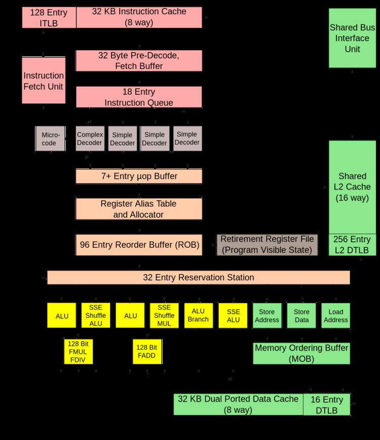
The Core microarchitecture returned to lower clock rates and improved the usage of both available clock cycles and power when compared with the preceding NetBurst microarchitecture of the Pentium 4/D-branded CPUs. The Core microarchitecture provides more efficient decoding stages, execution units, caches, and buses, reducing the power consumption of Core 2-branded CPUs while increasing their processing capacity. Intel's CPUs have varied widely in power consumption according to clock rate, architecture, and semiconductor process, shown in the CPU power dissipation tables.
Like the last NetBurst CPUs, Core based processors feature multiple cores and hardware virtualization support (marketed as Intel VT-x), as well as Intel 64 and SSSE3. However, Core-based processors do not have the Hyper-Threading Technology found in Pentium 4 processors. This is because the Core microarchitecture is a descendant of the P6 microarchitecture used by Pentium Pro, Pentium II, Pentium III, and Pentium M.
The L1 cache size was enlarged in the Core microarchitecture, from 32 KB on Pentium II/III (16 KB L1 Data + 16 KB L1 Instruction) to 64 KB L1 cache/core (32 KB L1 Data + 32 KB L1 Instruction) on Pentium M and Core/Core 2. It also lacks an L3 Cache found in the Gallatin core of the Pentium 4 Extreme Edition, although an L3 Cache is present in high-end versions of Core-based Xeons. Both an L3 cache and Hyper-threading were reintroduced in the Nehalem microarchitecture.
Technology
While the Core microarchitecture is a major architectural revision it is based in part on the Pentium M processor family designed by Intel Israel. The Penryn pipeline is 12–14 stages long — less than half of Prescott's, a signature feature of wide order execution cores. Penryn's successor, Nehalem borrowed more heavily from the Pentium 4 and has 20-24 pipeline stages. Core's execution unit is 4 issues wide, compared to the 3-issue cores of P6, Pentium M, and 2-issue cores of NetBurst microarchitectures. The new architecture is a dual core design with linked L1 cache and shared L2 cache engineered for maximum performance per watt and improved scalability.
One new technology included in the design is Macro-Ops Fusion, which combines two x86 instructions into a single micro-operation. For example, a common code sequence like a compare followed by a conditional jump would become a single micro-op. Unfortunately, this technology does not work in 64-bit mode.
Other new technologies include 1 cycle throughput (2 cycles previously) of all 128-bit SSE instructions and a new power saving design. All components will run at minimum speed, ramping up speed dynamically as needed (similar to AMD's Cool'n'Quiet power-saving technology, as well as Intel's own SpeedStep technology from earlier mobile processors). This allows the chip to produce less heat, and consume as little power as possible.
For most Woodcrest CPUs, the front side bus (FSB) runs at 1333 MT/s; however, this is scaled down to 1066 MT/s for lower end 1.60 and 1.86 GHz variants. The Merom mobile variant was initially targeted to run at a FSB of 667 MT/s while the second wave of Meroms, supporting 800 MT/s FSB, were released as part of the Santa Rosa platform with a different socket in May 2007. The desktop-oriented Conroe began with models having an FSB of 800 MT/s or 1066 MT/s with a 1333 MT/s line officially launched on July 22, 2007.
The power consumption of these new processors is extremely low—average use energy consumption is to be in the 1–2 watt range in ultra low voltage variants, with thermal design powers (TDPs) of 65 watts for Conroe and most Woodcrests, 80 watts for the 3.0 GHz Woodcrest, and 40 watts for the low-voltage Woodcrest. In comparison, an AMD Opteron 875HE processor consumes 55 watts, while the energy efficient Socket AM2 line fits in the 35 watt thermal envelope (specified a different way so not directly comparable). Merom, the mobile variant, is listed at 35 watts TDP for standard versions and 5 watts TDP for Ultra Low Voltage (ULV) versions.
Previously, Intel announced that it would now focus on power efficiency, rather than raw performance. However, at IDF in the spring of 2006, Intel advertised both. Some of the promised numbers were:
Processor cores
The processors of the Core microarchitecture can be categorized by number of cores, cache size, and socket; each combination of these has a unique code name and product code that is used across a number of brands. For instance, code name "Allendale" with product code 80557 has two cores, 2 MB L2 cache and uses the desktop socket 775, but has been marketed as Celeron, Pentium, Core 2 and Xeon, each with different sets of features enabled. Most of the mobile and desktop processors come in two variants that differ in the size of the L2 cache, but the specific amount of L2 cache in a product can also be reduced by disabling parts at production time. Wolfdale-DP and all quad-core processors except Dunnington QC are multi-chip modules combining two dies. For the 65 nm processors, the same product code can be shared by processors with different dies, but the specific information about which one is used can be derived from the stepping.
Conroe/Merom (65 nm)
The original Core 2 processors are based around the same dies that can be identified as CPUID Family 6 Model 15. Depending on their configuration and packaging, their code names are Conroe (LGA 775, 4 MB L2 cache), Allendale (LGA 775, 2 MB L2 cache), Merom (Socket M, 4 MB L2 cache) and Kentsfield (Multi-chip module, LGA 775, 2x4MB L2 cache). Merom and Allendale processors with limited features can be found in Pentium Dual Core and Celeron processors, while Conroe, Allendale and Kentsfield also are sold as Xeon processors.
Additional code names for processors based on this model are Woodcrest (LGA 771, 4 MB L2 cache), Clovertown (MCM, LGA 771, 2×4MB L2 cache) and Tigerton (MCM, Socket 604, 2×4MB L2 cache), all of which are marketed only under the Xeon brand.
Conroe-L/Merom-L
The Conroe-L and Merom-L processors are based around the same core as Conroe and Merom, but only contain a single core and 1 MB of L2 cache, significantly reducing production cost and power consumption of the processor at the expense of performance compared to the dual-core version. It is used only in ultra-low voltage Core 2 Solo U2xxx and in Celeron processors and is identified as CPUID family 6 model 22.
Penryn/Wolfdale (45 nm)
In Intel's Tick-Tock cycle, the 2007/2008 "Tick" was the shrink of the Core microarchitecture to 45 nanometers as CPUID model 23. In Core 2 processors, it is used with the code names Penryn (Socket P), Wolfdale (LGA 775) and Yorkfield (MCM, LGA 775), some of which are also sold as Celeron, Pentium and Xeon processors. In the Xeon brand, the Wolfdale-DP and Harpertown code names are used for LGA 771 based MCMs with two or four active Wolfdale cores.
The chips come in two sizes, with 6 MB and 3 MB L2 cache. The smaller version is commonly called Penryn-3M and Wolfdale-3M as well as Yorkfield-6M, respectively. The single-core version of Penryn, listed as Penryn-L here, is not a separate model like Merom-L but a version of the Penryn-3M model with only one active core.
Dunnington
The Xeon "Dunnington" processor (CPUID Family 6, model 29) is closely related to Wolfdale but comes with six cores and an on-chip L3 cache and is designed for servers with Socket 604, so it is marketed only as Xeon, not as Core 2.
Steppings
The Core microarchitecture uses a number of steppings, which unlike previous microarchitectures not only represent incremental improvements but also different sets of features like cache size and low power modes. Most of these steppings are used across brands, typically by disabling some of the features and limiting clock frequencies on low-end chips.
Steppings with a reduced cache size use a separate naming scheme, which means that the releases are no longer in alphabetic order. Additional steppings have been used in internal and engineering samples, but are not listed in the tables.
Many of the high-end Core 2 and Xeon processors use Multi-Chip Modules of two or three chips in order to get larger cache sizes or more than two cores.
Steppings using 65 nm process
Early ES/QS steppings are: B0 (CPUID 6F4h), B1 (6F5h) and E0 (6F9h).
Steppings B2/B3, E1 and G0 of model 15 (cpuid 06fx) processors are evolutionary steps of the standard Merom/Conroe die with 4 MiB L2 cache, with the short-lived E1 stepping only being used in mobile processors. Stepping L2 and M0 are the "Allendale" chips with just 2 MiB L2 cache, reducing production cost and power consumption for low-end processors.
The G0 and M0 steppings improve idle power consumption in C1E state and add the C2E state in desktop processors. In mobile processors, all of which support C1 through C4 idle states, steppings E1, G0, and M0 add support for the Mobile Intel 965 Express (Santa Rosa) platform with Socket P, while the earlier B2 and L2 steppings only appear for the Socket M based Mobile Intel 945 Express (Napa refresh) platform.
The model 22 stepping A1 (cpuid 10661h) marks a significant design change, with just a single core and 1 MiB L2 cache further reducing the power consumption and manufacturing cost for the low-end. Like the earlier steppings, A1 is not used with the Mobile Intel 965 Express platform.
Steppings G0, M0 and A1 mostly replaced all older steppings in 2008. In 2009, a new stepping G2 was introduced to replace the original stepping B2.
Steppings using 45 nm process
In the model 23 (cpuid 01067xh), Intel started marketing stepping with full (6 MiB) and reduced (3 MiB) L2 cache at the same time, and giving them identical cpuid values. All steppings have the new SSE4.1 instructions. Stepping C1/M1 was a bug fix version of C0/M0 specifically for quad core processors and only used in those. Stepping E0/R0 adds two new instructions (XSAVE/XRSTOR) and replaces all earlier steppings.
In mobile processors, stepping C0/M0 is only used in the Intel Mobile 965 Express (Santa Rosa refresh) platform, whereas stepping E0/R0 supports the later Intel Mobile 4 Express (Montevina) platform.
Model 30 stepping A1 (cpuid 106d1h) adds an L3 cache as well as six instead of the usual two cores, which leads to an unusually large die size of 503 mm². As of February 2008, it has only found its way into the very high-end Xeon 7400 series (Dunnington).
Motherboard compatibility
Conroe, Conroe XE and Allendale all use Socket LGA 775; however, not every motherboard is compatible with these processors.
Supporting chipsets are:
The currently released Yorkfield XE model QX9770 (45 nm with 1600 MT/s FSB) currently has limited chipset compatibility - with only X38, P35 (With Overclocking) and some high-performance X48 and P45 motherboards being compatible. BIOS updates are gradually being released to provide support for the new Penryn technology, and the new QX9775 is only compatible with the Intel D5400XS motherboard. The Wolfdale-3M model E7200 also has limited compatibility (at least the Xpress 200 chipset is incompatible).
Although a motherboard may have the required chipset to support Conroe, some motherboards based on the above-mentioned chipsets do not support Conroe. This is because all Conroe-based processors require a new power delivery feature set specified in Voltage Regulator-Down (VRD) 11.0. This requirement is a result of Conroe's significantly lower power consumption, compared to the Pentium 4/D CPUs it replaced. A motherboard that has both a supporting chipset and VRD 11 supports Conroe processors, but even then some boards will need an updated BIOS to recognize Conroe's FID (Frequency ID) and VID (Voltage ID).
Synchronous memory modules
Unlike the previous Pentium 4 and Pentium D design, the Core 2 technology sees a greater benefit from memory running synchronously with the Front Side Bus (FSB). This means that for the Conroe CPUs with FSB of 1066 MT/s, the ideal memory performance for DDR2 is PC2-8500. In a few configurations, using PC2-5300 instead of PC2-4200 can actually decrease performance. Only when going to PC2-6400 is there a significant performance increase. While DDR2 memory models with tighter timing specifications do improve performance, the difference in real world games and applications is often negligible.
Optimally, the memory bandwidth afforded should match the bandwidth of the FSB, that is to say that a CPU with a 533 MT/s rated bus speed should be paired with RAM matching the same rated speed, for example DDR2 533, or PC2-4200. A common myth is that installing interleaved RAM will offer double the bandwidth. However, at most the increase in bandwidth by installing interleaved RAM is roughly 5–10%. The AGTL+ PSB used by all NetBurst processors as well as current and medium-term (pre-QuickPath) Core 2 processors provide a 64-bit data path. Current chipsets provide for a couple of either DDR2 or DDR3 channels.
On jobs requiring large amounts of memory access, the quad-core Core 2 processors can benefit significantly from using PC2-8500 memory, which runs at exactly the same speed as the CPU's FSB; this is not an officially supported configuration, but a number of motherboards support it.
The Core 2 processor does not require the use of DDR2. While the Intel 975X and P965 chipsets require this memory, some motherboards and chipsets support both Core 2 processors and DDR memory. When using DDR memory, performance may be reduced because of the lower available memory bandwidth.
Chip errata
The Core 2 memory management unit (MMU) in X6800, E6000 and E4000 processors does not operate to previous specifications implemented in previous generations of x86 hardware. This may cause problems, many of them serious security and stability issues, with existing operating system software. Intel's documentation states that their programming manuals will be updated "in the coming months" with information on recommended methods of managing the translation lookaside buffer (TLB) for Core 2 to avoid issues, and admits that, "in rare instances, improper TLB invalidation may result in unpredictable system behavior, such as hangs or incorrect data."
Among the issues stated:
Intel errata Ax39, Ax43, Ax65, Ax79, Ax90, Ax99 are said to be particularly serious. 39, 43, 79, which can cause unpredictable behavior or system hang, have been fixed in recent steppings.
Among those who have stated the errata to be particularly serious are OpenBSD's Theo de Raadt and DragonFly BSD's Matthew Dillon. Taking a contrasting view was Linus Torvalds, calling the TLB issue "totally insignificant", adding, "The biggest problem is that Intel should just have documented the TLB behavior better."
Microsoft has issued update KB936357 to address the errata by microcode update, with no performance penalty. BIOS updates are also available to fix the issue.