
Produced From 1975 to 1990s Min. feature size 3 μm Transistors 6,500 | Max. CPU clock rate 3, 5 and 6 MHz Instruction set 80 | |
 | ||
Common manufacturer(s) Intel and several others | ||
The Intel 8085 ("eighty-eighty-five") is an 8-bit microprocessor produced by Intel and introduced in 1976. It is a software-binary compatible with the more-famous Intel 8080 with only two minor instructions added to support its added interrupt and serial input/output features. However, it requires less support circuitry, allowing simpler and less expensive microcomputer systems to be built.
Contents
- Description
- Programming model
- Commandsinstructions
- 8 bit instructions
- 16 bit operations
- Undocumented instructions
- Inputoutput scheme
- Development system
- Applications
- MCS 85 family
- Educational use
- Simulators
- References
The "5" in the part number highlighted the fact that the 8085 uses a single +5-volt (V) power supply by using depletion-mode transistors, rather than requiring the +5 V, −5 V and +12 V supplies needed by the 8080. This capability matched that of the competing Z80, a popular 8080-derived CPU introduced the year before. These processors could be used in computers running the CP/M operating system.
The 8085 is supplied in a 40-pin DIP package. To maximise the functions on the available pins, the 8085 uses a multiplexed address/data bus. However, an 8085 circuit requires an 8-bit address latch, so Intel manufactured several support chips with an address latch built in. These include the 8755, with an address latch, 2 KB of EPROM and 16 I/O pins, and the 8155 with 256 bytes of RAM, 22 I/O pins and a 14-bit programmable timer/counter. The multiplexed address/data bus reduced the number of PCB tracks between the 8085 and such memory and I/O chips.
Both the 8080 and the 8085 were eclipsed by the Zilog Z80 for desktop computers, which took over most of the CP/M computer market, as well as a share of the booming home-computer market in the early-to-mid-1980s.
The 8085 had a long life as a controller, no doubt thanks to its built-in serial I/O and 5 prioritized interrupts, arguably microcontroller-like features that the Z80 CPU did not have. Once designed into such products as the DECtape controller and the VT102 video terminal in the late 1970s, the 8085 served for new production throughout the lifetime of those products. This was typically longer than the product life of desktop computers.
Description
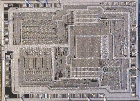
The 8085 is a conventional von Neumann design based on the Intel 8080. Unlike the 8080 it does not multiplex state signals onto the data bus, but the 8-bit data bus is instead multiplexed with the lower 8-bits of the 16-bit address bus to limit the number of pins to 40. State signals are provided by dedicated bus control signal pins and two dedicated bus state ID pins named S0 and S1. Pin 40 is used for the power supply (+5 V) and pin 20 for ground. Pin 39 is used as the Hold pin. The processor was designed using nMOS circuitry, and the later "H" versions were implemented in Intel's enhanced nMOS process called HMOS ("High-performance MOS"), originally developed for fast static RAM products. Only a single 5 volt power supply is needed, like competing processors and unlike the 8080. The 8085 uses approximately 6,500 transistors.
The 8085 incorporates the functions of the 8224 (clock generator) and the 8228 (system controller) on chip, increasing the level of integration. A downside compared to similar contemporary designs (such as the Z80) is the fact that the buses require demultiplexing; however, address latches in the Intel 8155, 8355, and 8755 memory chips allow a direct interface, so an 8085 along with these chips is almost a complete system.
The 8085 has extensions to support new interrupts, with three maskable vectored interrupts (RST 7.5, RST 6.5 and RST 5.5), one non-maskable interrupt (TRAP), and one externally serviced interrupt (INTR). Each of these five interrupts has a separate pin on the processor, a feature which permits simple systems to avoid the cost of a separate interrupt controller. The RST 7.5 interrupt is edge triggered (latched), while RST 5.5 and 6.5 are level-sensitive. All interrupts are enabled by the EI instruction and disabled by the DI instruction. In addition, the SIM (Set Interrupt Mask) and RIM (Read Interrupt Mask) instructions, the only instructions of the 8085 that are not from the 8080 design, allow each of the three maskable RST interrupts to be individually masked. All three are masked after a normal CPU reset. SIM and RIM also allow the global interrupt mask state and the three independent RST interrupt mask states to be read, the pending-interrupt states of those same three interrupts to be read, the RST 7.5 trigger-latch flip-flop to be reset (cancelling the pending interrupt without servicing it), and serial data to be sent and received via the SOD and SID pins, respectively, all under program control and independently of each other.
SIM and RIM each execute in 4 clock cycles (T states), making it possible to sample SID and/or toggle SOD considerably faster than it is possible to toggle or sample a signal via any I/O or memory-mapped port, e.g. one of the port of an 8155. (In this way, SID can be compared to the SO ["Set Overflow"] pin of the 6502 CPU contemporary to the 8085.)
Like the 8080, the 8085 can accommodate slower memories through externally generated wait states (pin 35, READY), and has provisions for Direct Memory Access (DMA) using HOLD and HLDA signals (pins 39 and 38). An improvement over the 8080 is that the 8085 can itself drive a piezoelectric crystal directly connected to it, and a built-in clock generator generates the internal high amplitude two-phase clock signals at half the crystal frequency (a 6.14 MHz crystal would yield a 3.07 MHz clock, for instance). The internal clock is available on an output pin, to drive peripheral devices or other CPUs in lock-step synchrony with the CPU from which the signal is output. The 8085 can also be clocked by an external oscillator (making it feasible to use the 8085 in synchronous multi-processor systems using a system-wide common clock for all CPUs, or to synchronize the CPU to an external time reference such as that from a video source or a high-precision time reference).
The 8085 is a binary compatible follow up on the 8080. It supports the complete instruction set of the 8080, with exactly the same instruction behavior, including all effects on the CPU flags (except for the AND/ANI operation, which sets the AC flag differently). This means that the vast majority of object code (any program image in ROM or RAM) that runs successfully on the 8080 can run directly on the 8085 without translation or modification. (Exceptions include timing-critical code and code that is sensitive to the aforementioned difference in the AC flag setting or differences in undocumented CPU behavior.) 8085 instruction timings differ slightly from the 8080—some 8-bit operations, including INR, DCR, and the heavily used MOV r,r' instruction, are 1 clock cycle faster, but instructions that involve 16-bit operations, including stack operations (which increment or decrement the 16-bit SP register) generally 1 cycle slower. It is of course possible that the actual 8080 and/or 8085 differs from the published specifications, especially in subtle details. (The same is not true of the Z80.) As mentioned already, only the SIM and RIM instructions were new to the 8085.
Programming model
The processor has seven 8-bit registers accessible to the programmer, named A, B, C, D, E, H, and L, where A is also known as the accumulator. The other six registers can be used as independent byte-registers or as three 16-bit register pairs, BC, DE, and HL (or B, D, H, as referred to in Intel documents), depending on the particular instruction. Some instructions use HL as a (limited) 16-bit accumulator. As in the 8080, the contents of the memory address pointed to by HL can be accessed as pseudo register M. It also has a 16-bit program counter and a 16-bit stack pointer to memory (replacing the 8008's internal stack). Instructions such as PUSH PSW, POP PSW affect the Program Status Word (accumulator and flags). The accumulator stores the results of arithmetic and logical operations, and the flags register bits (sign, zero, auxiliary carry, parity, and carry flags) are set or cleared according to the results of these operations. The sign flag is set if the result has a negative sign (i.e. it is set if bit 7 of the accumulator is set). The auxiliary or half carry flag is set if a carry-over from bit 3 to bit 4 occurred. The parity flag is set according to the parity (odd or even) of the accumulator. The zero flag is set if the result of the operation was 0. Lastly, the carry flag is set if a carry-over from bit 7 of the accumulator (the MSB) occurred.
Commands/instructions
As in many other 8-bit processors, all instructions are encoded in a single byte (including register-numbers, but excluding immediate data), for simplicity. Some of them are followed by one or two bytes of data, which can be an immediate operand, a memory address, or a port number. A NOP "no operation" instruction exists, but does not modify any of the registers or flags. Like larger processors, it has CALL and RET instructions for multi-level procedure calls and returns (which can be conditionally executed, like jumps) and instructions to save and restore any 16-bit register-pair on the machine stack. There are also eight one-byte call instructions (RST) for subroutines located at the fixed addresses 00h, 08h, 10h,...,38h. These are intended to be supplied by external hardware in order to invoke a corresponding interrupt-service routine, but are also often employed as fast system calls. One sophisticated instruction is XTHL, which is used for exchanging the register pair HL with the value stored at the address indicated by the stack pointer.
8-bit instructions
All 2-operand 8-bit arithmetic and logical (ALU) operations work on the 8-bit accumulator (the A register). For two-operand 8-bit operations, the other operand can be either an immediate value, another 8-bit register, or a memory cell addressed by the 16-bit register pair HL. The only 8-bit ALU operations that can have a destination other than the accumulator are the unary incrementation or decrementation instructions, which can operate on any 8-bit register or on memory addressed by HL, as for two-operand 8-bit operations. Direct copying is supported between any two 8-bit registers and between any 8-bit register and a HL-addressed memory cell, using the MOV instruction. An immediate value can also be moved into any of the foregoing destinations, using the MVI instruction. Due to the regular encoding of the MOV instruction (using nearly a quarter of the entire opcode space) there are redundant codes to copy a register into itself (MOV B,B, for instance), which are of little use, except for delays. However, what would have been a copy from the HL-addressed cell into itself (i.e., MOV M,M) instead encodes the HLT instruction, halting execution until an external reset or unmasked interrupt occurs.
16-bit operations
Although the 8085 is an 8-bit processor, it has some 16-bit operations. Any of the three 16-bit register pairs (BC, DE, HL or SP) can be loaded with an immediate 16-bit value (using LXI), incremented or decremented (using INX and DCX), or added to HL (using DAD). LHLD loads HL from directly addressed memory and SHLD stores HL likewise. The XCHG operation exchanges the values of HL and DE. Adding HL to itself performs a 16-bit arithmetical left shift with one instruction. The only 16 bit instruction that affects any flag is DAD (adding HL to BC, DE, HL or SP), which updates the carry flag to facilitate 24-bit or larger additions and left shifts. Adding the stack pointer to HL is useful for indexing variables in (recursive) stack frames. A stack frame can be allocated using DAD SP and SPHL, and a branch to a computed pointer can be done with PCHL. These abilities make it feasible to compile languages such as PL/M, Pascal, or C with 16-bit variables and produce 8085 machine code.
Subtraction and bitwise logical operations on 16 bits is done in 8-bit steps. Operations that have to be implemented by program code (subroutine libraries) include comparisons of signed integers as well as multiplication and division.
Undocumented instructions
A number of undocumented instructions and flags were discovered by two software engineers, Wolfgang Dehnhardt and Villy M. Sorensen in the process of developing an 8085 assembler. These instructions use 16-bit operands and include indirect loading and storing of a word, a subtraction, a shift, a rotate, and offset operations.
Input/output scheme
The 8085 supports up to 256 input/output (I/O) ports, accessed via dedicated Input/Output instructions—taking port addresses as operands. This I/O mapping scheme is regarded as an advantage, as it frees up the processor's limited address space. The IN and OUT instructions are used to read and write I/O port data. In an I/O bus cycle, the 8-bit I/O address is output by the CPU on both the lower and upper halves of the 16-bit address bus.
Memory mapped I/O devices can also be accessed by using the LDA (load accumulator from a 16-bit address) and STA (store accumulator at a 16-bit address specified) instructions, or any other instructions that have memory operands.
Development system
Intel produced a series of development systems for the 8080 and 8085, known as the MDS-80 Microprocessor System. The original development system had an 8080 processor. Later 8085 and 8086 support was added including ICE (in-circuit emulators). It is a large and heavy desktop box, about a 20" cube (in the Intel corporate blue color) which includes a CPU, monitor, and a single 8-inch floppy disk drive. Later an external box was made available with two more floppy drives. It runs the ISIS operating system and can also operate an emulator pod and an external EPROM programmer. This unit uses the Multibus card cage which was intended just for the development system. A surprising number of spare card cages and processors were being sold, leading to the development of the Multibus as a separate product.
The later iPDS is a portable unit, about 8" x 16" x 20", with a handle. It has a small green screen, a keyboard built into the top, a 5¼ inch floppy disk drive, and runs the ISIS-II operating system. It can also accept a second 8085 processor, allowing a limited form of multi-processor operation where both processors run simultaneously and independently. The screen and keyboard can be switched between them, allowing programs to be assembled on one processor (large programs took awhile) while files are edited in the other. It has a bubble memory option and various programming modules, including EPROM, and Intel 8048 and 8051 programming modules which are plugged into the side, replacing stand-alone device programmers. In addition to an 8080/8085 assembler, Intel produced a number of compilers including those for PL/M-80 and Pascal, and a set of tools for linking and statically locating programs to enable them to be burned into EPROMs and used in embedded systems.
A lower cost SDK-85 System Design Kit board contains an 8085 CPU, an 8355 ROM containing a debugging monitor program, an 8155 RAM and 22 I/O ports, an 8279 hex keypad and 8-digit 7-segment LED, and a TTY (Teletype) 20 mA current loop serial interface. Pads are available for one more 2K×8 8755 EPROM, and another 256 byte RAM 8155 I/O Timer/Counter can be optionally added. All data, control, and address signals are available on dual pin headers, and a large prototyping area is provided.
Applications
For the extensive use of 8085 in various applications, the microprocessor is provided with an instruction set consisting of various instructions such as MOV, ADD, SUB, JMP, etc. These instructions are written in the form of a program which is used to perform various operations such as branching, addition, subtraction, bitwise logical, and bit shift operations. More complex operations and other arithmetic operations must be implemented in software. For example, multiplication is implemented using a multiplication algorithm.
The 8085 processor was used in a few early personal computers, for example, the TRS-80 Model 100 line used an OKI manufactured 80C85 (MSM80C85ARS). The CMOS version 80C85 of the NMOS/HMOS 8085 processor has several manufacturers. In the Soviet Union, an 80C85 clone was developed under the designation IM1821VM85A (Russian: ИМ1821ВМ85А) which in 2016 was still in production. Some manufacturers provide variants with additional functions such as additional instructions. The rad-hard version of the 8085 has been in on-board instrument data processors for several NASA and ESA space physics missions in the 1990s and early 2000s, including CRRES, Polar, FAST, Cluster, HESSI, the Sojourner Mars Rover, and THEMIS. The Swiss company SAIA used the 8085 and the 8085-2 as the CPUs of their PCA1 line of programmable logic controllers during the 1980s.
Pro-Log Corp. put the 8085 and supporting hardware on an STD Bus format card containing CPU, RAM, sockets for ROM/EPROM, I/O and external bus interfaces. The included Instruction Set Reference Card uses entirely different mnemonics for the Intel 8085 CPU, as the product was a direct competitor to Intel's Multibus card offerings.
MCS-85 family
The 8085 CPU is one part of a family of chips developed by Intel, for building a complete system. Many of these support chips were also used with other processors. The original IBM PC based on the Intel 8088 processor used several of these chips; the equivalent functions today are provided by VLSI chips, namely the "Southbridge" chips.
Educational use
In many engineering schools the 8085 processor is used in introductory microprocessor courses. Trainer kits composed of a printed circuit board, 8085, and supporting hardware are offered by various companies. These kits usually include complete documentation allowing a student to go from soldering to assembly language programming in a single course. Also, the architecture and instruction set of the 8085 are easy for a student to understand.
Simulators
Some of the simulators available for the 8085 microprocessor are listed below: