
Produced From 2007 to 2012 Max. CPU clock rate 1700 MHz to 3700 MHz Min. feature size 65 nm to 45 nm | Common manufacturer(s) AMD FSB speeds 1000 MHz to 2000 MHz | |
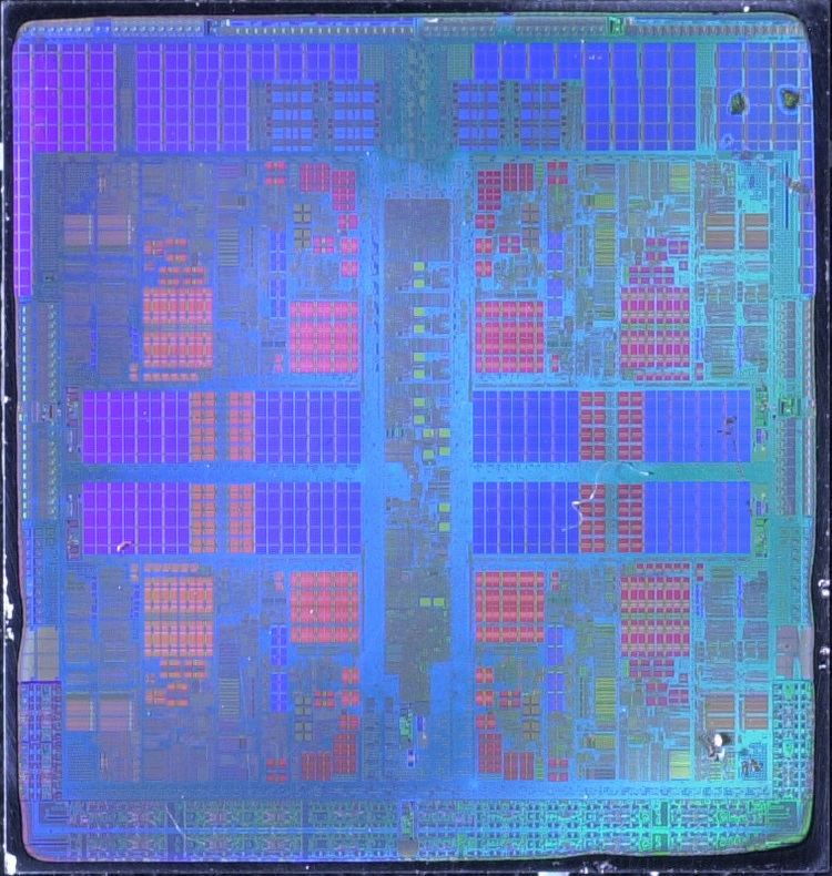 | ||
The AMD Family 10h, or K10, is a microprocessor microarchitecture by AMD based on the K8 microarchitecture. Though there were once reports that the K10 had been canceled, the first third-generation Opteron products for servers were launched on September 10, 2007, with the Phenom processors for desktops following and launching on November 11, 2007 as the immediate successors to the K8 series of processors (Athlon 64, Opteron, 64-bit Sempron).
Contents
- Nomenclatures
- Historical information
- Confirmation of time frames
- TLB Bug
- Internal codenames
- Subsequent product launches
- Change of model nomenclatures
- Live demonstrations
- Sister microarchitecture
- Iterations of the release
- Fabrication technology
- Supported DRAM standards
- Higher computational throughput
- Microarchitecture characteristics
- Agena 65 nm SOI
- Toliman 65 nm SOI
- Thuban 45 nm SOI with Immersion Lithography
- Deneb 45 nm SOI with Immersion Lithography
- Heka 45 nm SOI with Immersion Lithography
- Callisto 45 nm SOI with Immersion Lithography
- Regor 45 nm SOI with Immersion Lithography
- Successor
- Turion X2 Ultra Family 11h
- Fusion Family 12h
- Media discussions
- References
Nomenclatures
It is commonly perceived by the PC community that from the time after the use of the codename K8 for the AMD K8 or Athlon 64 processor family, AMD no longer uses K-nomenclatures (originally stood for Kryptonite) since no K-nomenclature naming convention beyond K8 has appeared in official AMD documents and press releases after the beginning of 2005.
The name "K8L" was first coined by Charlie Demerjian, one of the writers of The Inquirer back in 2005, and was used by the wider IT community as a convenient shorthand while according to AMD official documents, the processor family was termed "AMD Next Generation Processor Technology".
The microarchitecture has also been referred to as Stars, as the codenames for desktop line of processors was named under stars or constellations (the initial Phenom models being codenamed Agena and Toliman).
In a video interview, Giuseppe Amato confirmed that the codename is K10.
It was revealed, by The Inquirer itself, that the codename "K8L" referred to a low-power version of the K8 family, later named Turion 64, and that K10 was the official codename for the microarchitecture.
AMD refers to it as Family 10h Processors, as it is the successor of the Family 0Fh Processors (codename K8). 10h and 0Fh refer to the main result of the CPUID x86 processor instruction. In hexadecimal numbering, 0Fh (h represents hexadecimal numbering) equals the decimal number 15, and 10h equals decimal 16. (The "K10h" form that sometimes pops up is an improper hybrid of the "K" code and Family identifier number.)
Historical information
In 2003, AMD outlined the features for upcoming generations of microprocessors after the K8 family of processors in various events and analyst meetings, including the Microprocessor Forum 2003. The outlined features to be deployed by the next-generation microprocessors are as follows:
On April 13, 2006, Henri Richard, AMD executive vice president and chief officer for marketing and sales, acknowledged the existence of the new microarchitecture in an interview.
In June 2006, AMD executive vice president Henri Richard had another interview with DigiTimes commented on the upcoming processor developments:
Q: What is your broad perspective on the development of AMD processor technology over the next three to four years? A: Well, as Dirk Meyer commented at our analysts meeting, we're not standing still. We've talked about the refresh of the current K8 architecture that will come in '07, with significant improvements in many different areas of the processor, including integer performance, floating point performance, memory bandwidth, interconnections and so on.
Confirmation of time frames
On July 21, 2006, AMD President and Chief operating officer (COO) Dirk Meyer and Senior VP Marty Seyer confirmed that the launch date of new microprocessors of Revision H under the new microarchitecture is slated for the middle of 2007; and that it will contain a quad core version for servers, workstations, and high-end desktops, as well as a dual core version for consumer Desktops. Some of the Revision H Opterons shipped in 2007 will have a thermal design power of 68 W.
On August 15, 2006, at the launch of the first Socket F dual-core Opterons, AMD announced that the firm had reached the final design stage (tape-out) of quad-core Opteron parts. The next stages are testing and validation, with sampling to follow after several months.
On June 29, 2007, AMD stated that server processors codenamed Barcelona will ship in August 2007, and corresponding server systems from partners will ship in September of the same year.
On August 13, the reported ship dates for the first Barcelona processors were set for September 10, 2007. They announced the Opteron 2348 and 2350 will have core frequencies of 1.9 GHz and 2.0 GHz.
TLB Bug
In November 2007 AMD stopped delivery of Barcelona processors after a bug in the translation lookaside buffer (TLB) of stepping B2 was discovered that could rarely lead to a race condition and thus a system lockup. A patch in BIOS or software worked around the bug by disabling cache for page tables, but it was connected to a 5 to 20% performance penalty. Kernel patches that would almost completely avoid this penalty were published for Linux. In April 2008, the new stepping B3 was brought to the market by AMD, including a fix for the bug plus other minor enhancements.
Internal codenames
As of November 2006, reports leaked the upcoming desktop part codenames Agena, Agena FX, and the core speeds of the parts range from 2.4 GHz - 2.9 GHz respectively, 512 KB L2 cache each core, 2 MB L3 cache, using HyperTransport 3.0, with a TDP of 125 W. In recent reports, single core variants (codenamed Spica) and dual core with or without L3 cache (codenamed Kuma and Rana respectively) are available under the same microarchitecture.
During the AMD Analyst Day 2006 on December 14, 2006, AMD announced their official timeline for server, desktop and mobile processors. For the servers segment, AMD will unveil two new processors based on the architecture codenamed "Barcelona" and "Budapest" for 8/4/2-way and 1-way servers respectively. For the second half of 2007, HyperTransport 3.0 and Socket AM2+ will be unveiled, which are designed for the specific implementation of the aforementioned consumer quad core desktop chip series, with naming convention changes from city names (up to middle of 2007) to stars or constellations after that, such as Agena; in addition, the AMD Quad FX platform and its immediate successor will support the high end enthusiast dual-processor versions of the chip, codenamed as Agena FX, updates the processors line for AMD Quad FX platform. As with the server chips codenamed Barcelona, the new desktop quad core series will feature a shared L3 cache, 128-bit floating point (FP) units and an enhanced microarchitecture. Agena will be the native quad-core processor for the desktop. Kuma, a dual-core variant will follow on in Q3 while Rana, the dual-core version with no shared L3 cache is expected at the end of the year.
Subsequent product launches
More information about the upcoming chip codenamed "Montreal" on the server roadmap using MCM technique of two "Shanghai" cores with a total of 12 MB L3 cache codenamed AMD K10.5. The desktop variant for Shanghai is codenamed Ridgeback. Afterwards is the release of products based on the Bulldozer cores, which is optimized with integrated graphics core (AMD Accelerated Processing Unit) or native octal-core (8 core) server architecture (codenamed Sandtiger), and the Bobcat core, optimized for low-power operations.
Change of model nomenclatures
During Computex 2007 in early June, new information regarding the naming schemes of upcoming AMD microprocessors emerged. Additional letters indicating both performance and power envelope will precede the 4 digit model number.
The model numbers of the new line of processors were apparently changed from the PR ratings used by its predecessors, the Athlon 64 series processors (except Phenom FX series, being suggested to follow the nomenclature of Athlon 64 FX series). As reported by DailyTech, the model numbers are in alpha-numeric format as AA-@### where AA are alphabetical letters, the first letter indicating the processor class and the second indicating the typical TDP power envelope. The character @ is the series indicator, which varies by branding (see below table), and the last three characters (###) are the model number, with higher numbers indicating greater performance.
Not much information was known about the details of the model numbers, but the processors will be divided into three segments: Premium, Intermediate, and Value. Premium segment model numbers have processor class "G", Intermediate segment "B", and Value level "L", as discovered on the web from the AsRock website. Similarly, three levels of TDP, "more than 65W", "65W", and "less than 65W", are indicated by the letters "P", "S", and "E" respectively.
As of November 2007, AMD has removed the letters from the model names and X2/X3/X4 monikers for depicting the number of cores of the processor, leaving just a four digit model number with the first character being the sole identification of the processor family, while Sempron remained using the LE prefix, as follows:
Live demonstrations
On November 30, 2006, AMD live demonstrated the native quad core chip known as "Barcelona" for the first time in public, while running Windows Server 2003 64-bit Edition. AMD claims 70% scaling of performance in real world loads, and better performance than Intel Xeon 5355 processor codenamed Clovertown. More details regarding this first revision of the next generation AMD microprocessor architecture have surfaced on the web including their clock speeds.
On January 24, 2007, AMD Executive Vice President Randy Allen claimed that in live tests, in regard to a wide variety of workloads, "Barcelona" was able to demonstrate 40% performance advantage over the comparable Intel Xeon codenamed Clovertown dual-processor (2P) quad-core processors. The expected performance of floating point per core would be approximately 1.8 times that of the K8 family, at the same clock speed.
On May 10, 2007, AMD held a private event demonstrating the upcoming processors codenamed Agena FX and chipsets, with one demonstrated system being AMD Quad FX platform with one Radeon HD 2900 XT graphics card on the upcoming RD790 chipset, the system was also demonstrated real-time converting a 720p video clip into another undisclosed format while all 8 cores were maxed at 100% by other tasks.
Sister microarchitecture
Also due in a similar time frame will be a sister microarchitecture, which will focus on lower power consumption chips in mobile platforms as well as small form factor features. This microarchitecture will contain specialized features such as mobile optimized crossbar switch and memory controller and other on-die components; link power management for HyperTransport 3.0; and others. At that time, AMD simply dubbed it "New Mobile Core", without giving a specific codename.
On the December 2006 analyst day, Executive vice president Marty Seyer announced the new mobile core codenamed Griffin launched in 2008 with inherited power optimizations technologies from the K10 microarchitecture, but based on a K8 design
Iterations of the release
In late 2007 to second quarter of 2008, there will be a modification to the core to be fabricated at 45 nm process node, with enhancements such as FB-DIMM support, Direct Connect Architecture 2.0, enhanced Reliability, Availability and Serviceability (RAS), and probably more for the processor die. The platform will also add support for I/O Virtualization, PCI Express 2.0, 10 Gigabit NIC, larger caches, and more.
However, reports have suggested that FB-DIMM support had been dropped from future roadmaps of the majority of AMD products since popularity is low. Also, FB-DIMM's future as an industry standard had been called into question.
An article published by The Inquirer corroborates the earlier reports of the timeline (as cited in this article). According to the report, there will be three iterations of the server processor core: one named Barcelona, due in Q2 of 2007, with new CPU core components as well as the microarchitecture, but built on the old HyperTransport 2.0 infrastructure; the second is Budapest for single socket systems using socket AM2+ or socket AM3, with HyperTransport 3.0; and the third, codenamed Shanghai is an update of the server chip, based on 45 nm process, probably also with HyperTransport 3.0 and DDR3 implementation, due in Q1-Q2 2008.
AMD, on September 17, 2007, announced that a three core (triple-core) processor will also be released under the Phenom brand lineup, codenamed Toliman. AMD official replied in an interview that this product is benefitted from ATI technologies to add fuses to the quad-core processor and shutting down one of the four cores to become a triple-core processor, which the technique has been popular for making one or more mainstream GPU cores from a single high-end GPU core by blowing out parts of the circuit to save R&D costs while targeting more markets some time ago. The triple-core processor still see the same specifications for quad-core variants, the naming of the processor lineup, according to the AMD branding scheme, will be named as Phenom triple-core 8000 series, the processor line will be focused on what AMD called the fourth market segment or the "High-end Mainstream" segment beside Value, Mainstream and Performance segments in an interview with BetaNews, which the targeted customers of the processors are "those who are willing to pay more for more performance but not required for too much processing power as required by gamers and system builders", while there are single core (Sempron) variants for low-end market, and dual-core (Athlon) variants for mid-range market, and quad-core (Phenom quad-core 9000 series and Phenom FX) variants should be seen in the high-end market at the same time frame.
Further in 2008, AMD will introduce Deneb FX for the replacement for the AMD Quad FX platform, as well as Deneb for the mainstream. Propos and Regor will also replace Kuma and Rana in the lower market segments. Socket AM2+ being named in the late 2006 might actually have been the original AM3 socket, but as naming conventions changed, so that the next generation of consumer desktop socket capable of DDR3 will be socket AM3.
Fabrication technology
AMD has introduced the microprocessors manufactured at 65 nm feature width using Silicon-on-insulator (SOI) technology, since the release of K10 coincides with the volume ramp of this manufacturing process. The servers will be produced for Socket F(1207) or later 1207-pin socket infrastructure, the only server socket on AMD's near-term roadmap; the desktop parts will come on Socket AM2 or Socket AM2+.
AMD announced during the Technology Analyst Day that the use of Continuous Transistor Improvement (CTI) and Shared Transistor Technology (STT) would finally lead to the implementation of Silicon-Germanium-On-Insulator (SGoI) on 65 nm process CPUs.
Supported DRAM standards
The K8 family was known to be particularly sensitive to memory latency since its design gains performance by minimizing this through the use of an on-die memory controller (integrated into the CPU); increased latency in the external modules negates the usefulness of the feature. DDR2 RAM introduces some additional latency over traditional DDR RAM since the DRAM is internally driven by a clock at one quarter of the external data frequency, as opposed to one half that of DDR. However, since the command clock rate in DDR2 is doubled relative to DDR and other latency-reducing features (e.g. additive latency) have been introduced, common comparisons based on CAS latency alone are not sufficient. For example, Socket AM2 processors are known to demonstrate similar performance using DDR2 SDRAM as Socket 939 processors that utilize DDR-400 SDRAM. K10 processors support DDR2 SDRAM rated up to DDR2-1066 (1066 MHz).
Higher computational throughput
It was also reported by several sources (such as AnandTech, The Inquirer and Geek.com) that the microprocessors implementing the microarchitecture will feature a doubling in the width of SSE execution units in the cores. With the help of major improvements in the memory subsystem (such as load re-ordering and improved prefetch mechanisms) as well as the doubled instruction fetch and load, it is expected to increase the suitability of the processor to scientific and high-performance computing tasks and potentially improve its competitiveness with Intel's Xeon, Core 2, Itanium 2 and other contemporary microprocessors.
Many of the improvements in computational throughput of each core are listed below.
Microarchitecture characteristics
Characteristics of the microarchitecture include the following:
Agena (65 nm SOI)
Toliman (65 nm SOI)
Thuban (45 nm SOI with Immersion Lithography)
Deneb (45 nm SOI with Immersion Lithography)
Heka (45 nm SOI with Immersion Lithography)
Callisto (45 nm SOI with Immersion Lithography)
Regor (45 nm SOI with Immersion Lithography)
Successor
AMD discontinued further development of K10 based CPUs after Thuban, choosing to focus on Fusion products for mainstream desktops and laptops and Bulldozer based products for the performance market. However, within the Fusion product family, APUs such as the first generation A4, A6 and A8-series chips (Llano APUs) continued to use K10-derived CPU cores in conjunction with a Radeon graphics core. K10 and its derivatives were phased out of production by the introduction of Trinity-based APUs in 2012, which replaced the K10 cores in the APU with Bulldozer-derived cores.
Turion X2 Ultra Family 11h
The Family 11h microarchitecture was a mixture of both K8 and K10 designs with lower power consumption for laptop that was marketed as Turion X2 Ultra and was later replaced by completely K10-based designs.
Fusion Family 12h
The Family 12h microarchitecture is a derivative of the K10 design:
Media discussions
Note: These media discussions are listed in ascending date of publication.