
 | ||
Wafer-scale integration, WSI for short, is a rarely used system of building very-large integrated circuit networks that use an entire silicon wafer to produce a single "super-chip". Combining large size and reduced packaging, WSI was expected to lead to dramatically reduced costs for some systems, notably massively parallel supercomputers. The name is taken from the term very-large-scale integration, the current state of the art when WSI was being developed.
Contents
The concept
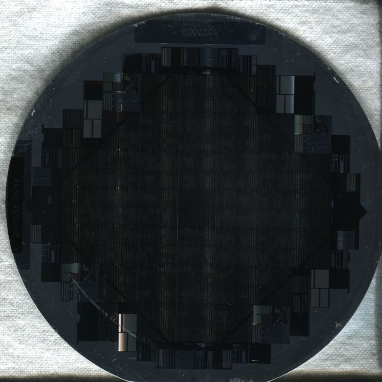
To understand WSI, one has to consider the normal chip-making process. A single large cylindrical crystal of silicon is produced and then cut into disks known as wafers. The wafers are then cleaned and polished in preparation for the fabrication process. A photographic process is used to pattern the surface where material ought to be deposited on top of the wafer and where not to. The desired material is deposited and the photographic mask is removed for the next layer. From then on the wafer is repeatedly processed in this fashion, putting on layer after layer of circuitry on the surface.
Multiple copies of these patterns are deposited on the wafer in a grid fashion across the surface of the wafer. After all the possible locations are patterned, the wafer surface appears like a sheet of graph paper, with grid lines delineating the individual chips. Each of these grid locations is tested for manufacturing defects by automated equipment. Those locations that are found to be defective are recorded and marked with a dot of paint (this process is referred to as "inking a die" however modern wafer fabrication no longer requires physical markings to identify defective die). The wafer is then sawed apart to cut out the individual chips. Those defective chips are thrown away, or recycled, while the working chips are placed into packaging and re-tested for any damage that might occur during the packaging process.
Flaws on the surface of the wafers and problems during the layering/depositing process are impossible to avoid, and cause some of the individual chips to be defective. The revenue from the remaining working chips has to pay for the entire cost of the wafer and its processing, including those discarded defective chips. Thus, the higher number of working chips or higher yield, the lower the cost of each individual chip. In order to maximize yield one wants to make the chips as small as possible, so that a higher number of working chips can be obtained per wafer.
The vast majority of the cost of fabrication (typically 30%-50%) is related to testing and packaging the individual chips. Further cost is associated with connecting the chips into an integrated system (usually via a printed circuit board). Wafer-scale integration seeks to reduce this cost, as well as improve performance, by building larger chips in a single package – in principle, chips as large as a full wafer.
Of course this is not easy, since given the flaws on the wafers a single large design printed onto a wafer would almost always not work. It has been an ongoing goal to develop methods to handle faulty areas of the wafers through logic, as opposed to sawing them out of the wafer. Generally, this approach uses a grid pattern of sub-circuits and "rewires" around the damaged areas using appropriate logic. If the resulting wafer has enough working sub-circuits, it can be used despite faults.
Production attempts
Many companies attempted to develop WSI production systems in the 1970s and 80s, but all failed. TI and ITT both saw it as a way to develop complex pipelined microprocessors and re-enter a market where they were losing ground, but neither released any products.
Gene Amdahl also attempted to develop WSI as a method of making a supercomputer, starting Trilogy Systems in 1980 and garnering investments from Groupe Bull, Sperry Rand and Digital Equipment Corporation, who (along with others) provided an estimated $230 million in financing. The design called for a 2.5" square chip with 1200 pins on the bottom.
The effort was plagued by a series of disasters, including floods which delayed the construction of the plant and later ruined the clean-room interior. After burning through about 1/3 of the capital with nothing to show for it, Amdahl eventually declared the idea would only work with a 99.99% yield, which wouldn't happen for 100 years. He used Trilogy's remaining seed capital to buy Elxsi, a maker of VAX-compatible computers, in 1985. The Trilogy efforts were eventually ended and "became" Elxsi.