
 | ||
A thin-film solar cell is a second generation solar cell that is made by depositing one or more thin layers, or thin film (TF) of photovoltaic material on a substrate, such as glass, plastic or metal. Thin-film solar cells are commercially used in several technologies, including cadmium telluride (CdTe), copper indium gallium diselenide (CIGS), and amorphous thin-film silicon (a-Si, TF-Si).
Contents
- History
- Materials
- Cadmium telluride
- Copper indium gallium selenide
- Amorphous silicon
- Amorphous silicon cells
- Tandem cell using a Sic Si
- Tandem cell using a Sipc Si
- Polycrystalline silicon on glass
- Gallium arsenide thin film cells
- Emerging photovoltaics
- Efficiencies
- Absorption
- Production cost and market
- Market share
- CIGS technology
- CdTe technology
- a Si technology
- Awards
- References
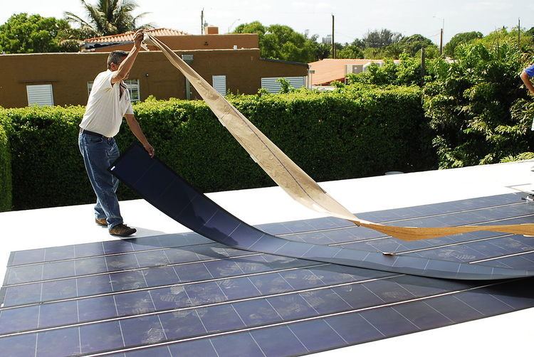
Film thickness varies from a few nanometers (nm) to tens of micrometers (µm), much thinner than thin-film's rival technology, the conventional, first-generation crystalline silicon solar cell (c-Si), that uses wafers of up to 200 µm. This allows thin film cells to be flexible, and lower in weight. It is used in building integrated photovoltaics and as semi-transparent, photovoltaic glazing material that can be laminated onto windows. Other commercial applications use rigid thin film solar panels (sandwiched between two panes of glass) in some of the world's largest photovoltaic power stations.
Thin-film technology has always been cheaper but less efficient than conventional c-Si technology. However, it has significantly improved over the years. The lab cell efficiency for CdTe and CIGS is now beyond 21 percent, outperforming multicrystalline silicon, the dominant material currently used in most solar PV systems. Accelerated life testing of thin film modules under laboratory conditions measured a somewhat faster degradation compared to conventional PV, while a lifetime of 20 years or more is generally expected. Despite these enhancements, market-share of thin-film never reached more than 20 percent in the last two decades and has been declining in recent years to about 9 percent of worldwide photovoltaic installations in 2013.
Other thin-film technologies that are still in an early stage of ongoing research or with limited commercial availability are often classified as emerging or third generation photovoltaic cells and include organic, dye-sensitized, and polymer solar cells, as well as quantum dot, copper zinc tin sulfide, nanocrystal, micromorph, and perovskite solar cells.
History
Thin film cells are well-known since the late 1970s, when solar calculators powered by a small strip of amorphous silicon appeared on the market.
It is now available in very large modules used in sophisticated building-integrated installations and vehicle charging systems.
Although thin-film technology was expected to make significant advances in the market and to surpass the dominating conventional crystalline silicon (c-Si) technology in the long-term, market-share has been declining for several years now. While in 2010, when there was a shortage of conventional PV modules, thin-film accounted for 15 percent of the overall market, it declined to 8 percent in 2014, and is expected to stabilize at 7 percent from 2015 onward, with amorphous silicon expected to lose half of its market-share by the end of the decade.
Materials
Thin-film technologies reduce the amount of active material in a cell. Most sandwich active material between two panes of glass. Since silicon solar panels only use one pane of glass, thin film panels are approximately twice as heavy as crystalline silicon panels, although they have a smaller ecological impact (determined from life cycle analysis). The majority of film panels have 2-3 percentage points lower conversion efficiencies than crystalline silicon. Cadmium telluride (CdTe), copper indium gallium selenide (CIGS) and amorphous silicon (a-Si) are three thin-film technologies often used for outdoor applications.
Cadmium telluride
Cadmium telluride (CdTe) is the predominant thin film technology. With about 5 percent of worldwide PV production, it accounts for more than half of the thin film market. The cell's lab efficiency has also increased significantly in recent years and is on a par with CIGS thin film and close to the efficiency of multi-crystalline silicon as of 2013. Also, CdTe has the lowest Energy payback time of all mass-produced PV technologies, and can be as short as eight months in favorable locations. A prominent manufacturer is the US-company First Solar based in Tempe, Arizona, that produces CdTe-panels with an efficiency of about 14 percent at a reported cost of $0.59 per watt.
Although the toxicity of cadmium may not be that much of an issue and environmental concerns completely resolved with the recycling of CdTe modules at the end of their life time, there are still uncertainties and the public opinion is skeptical towards this technology. The usage of rare materials may also become a limiting factor to the industrial scalability of CdTe thin film technology. The rarity of tellurium—of which telluride is the anionic form—is comparable to that of platinum in the earth's crust and contributes significantly to the module's cost.
Copper indium gallium selenide
A copper indium gallium selenide solar cell or CIGS cell uses an absorber made of copper, indium, gallium, selenide (CIGS), while gallium-free variants of the semiconductor material are abbreviated CIS. It is one of three mainstream thin-film technologies, the other two being cadmium telluride and amorphous silicon, with a lab-efficiency above 20 percent and a share of 2 percent in the overall PV market in 2013. A prominent manufacturer of cylindrical CIGS-panels was the now-bankrupt company Solyndra in Fremont, California. Traditional methods of fabrication involve vacuum processes including co-evaporation and sputtering. In 2008, IBM and Tokyo Ohka Kogyo Co., Ltd. (TOK) announced they had developed a new, non-vacuum, solution-based manufacturing process for CIGS cells and are aiming for efficiencies of 15% and beyond.
Hyperspectral imaging has been used to characterize these cells. Researchers from IRDEP (Institute of Research and Development in Photovoltaic Energy) in collaboration with Photon etc.¸ were able to determine the splitting of the quasi-Fermi level with photoluminescence mapping while the electroluminescence data were used to derive the external quantum efficiency (EQE). Also, through a light beam induced current (LBIC) cartography experiment, the EQE of a microcrystalline CIGS solar cell could be determined at any point in the field of view.
As of September 2014, current conversion efficiency record for a laboratory CIGS cell stands at 21.7%.
Amorphous silicon
Amorphous silicon (a-Si) is a non-crystalline, allotropic form of silicon and the most well-developed thin film technology to-date. Thin-film silicon is an alternative to conventional wafer (or bulk) crystalline silicon. While chalcogenide-based CdTe and CIS thin films cells have been developed in the lab with great success, there is still industry interest in silicon-based thin film cells. Silicon-based devices exhibit fewer problems than their CdTe and CIS counterparts such as toxicity and humidity issues with CdTe cells and low manufacturing yields of CIS due to material complexity. Additionally, due to political resistance to the use non-"green" materials in solar energy production, there is no stigma in the use of standard silicon.
Three major silicon-based module designs dominate:
Amorphous silicon cells
This type of thin-film cell is mostly fabricated by a technique called plasma-enhanced chemical vapor deposition. It uses a gaseous mixture of silane (SiH4) and hydrogen to deposit a very thin layer of only 1 micrometre (µm) of silicon on a substrate, such as glass, plastic or metal, that has already been coated with a layer of transparent conducting oxide. Other methods used to deposit amorphous silicon on a substrate include sputtering and hot wire chemical vapor deposition techniques.
a-Si is attractive as a solar cell material because it's an abundant, non-toxic material. It requires a low processing temperature and enables a scalable production upon a flexible, low-cost substrate with little silicon material required. Due to its bandgap of 1.7 eV, amorphous silicon also absorbs a very broad range of the light spectrum, that includes infrared and even some ultraviolet and performs very well at weak light. This allows the cell to generate power in the early morning, or late afternoon and on cloudy and rainy days, contrary to crystalline silicon cells, that are significantly less efficient when exposed at diffuse and indirect daylight.
However, the efficiency of an a-Si cell suffers a significant drop of about 10 to 30 percent during the first six months of operation. This is called the Staebler-Wronski effect (SWE) – a typical loss in electrical output due to changes in photoconductivity and dark conductivity caused by prolonged exposure to sunlight. Although this degradation is perfectly reversible upon annealing at or above 150 °C, conventional c-Si solar cells do not exhibit this effect in the first place.
Its basic electronic structure is the p-i-n junction. The amorphous structure of a-Si implies high inherent disorder and dangling bonds, making it a bad conductor for charge carriers. These dangling bonds act as recombination centers that severely reduce carrier lifetime. A p-i-n structure is usually used, as opposed to an n-i-p structure. This is because the mobility of electrons in a-Si:H is roughly 1 or 2 orders of magnitude larger than that of holes, and thus the collection rate of electrons moving from the n- to p-type contact is better than holes moving from p- to n-type contact. Therefore, the p-type layer should be placed at the top where the light intensity is stronger, so that the majority of the charge carriers crossing the junction are electrons.
Tandem-cell using a-Si/μc-Si
A layer of amorphous silicon can be combined with layers of other allotropic forms of silicon to produce a multi-junction solar cell. When only two layers (two p-n junctions) are combined, it is called a tandem-cell. By stacking these layers on top of one other, a broader range of the light spectra is absorbed, improving the cell's overall efficiency.
In micromorphous silicon, a layer of microcrystalline silicon (μc-Si) is combined with amorphous silicon, creating a tandem cell. The top a-Si layer absorbs the visible light, leaving the infrared part to the bottom μc-Si layer. The micromorph stacked-cell concept was pioneered and patented at the Institute of Microtechnology (IMT) of the Neuchâtel University in Switzerland, and is currently licensed to TEL Solar. A new world record PV module based on the micromorph concept with 12.24% module efficiency was independently certified in July 2014.
Because all layers are made of silicon, they can be manufactured using PECVD. The band gap of a-Si is 1.7 eV and that of c-Si is 1.1 eV. The c-Si layer can absorb red and infrared light. The best efficiency can be achieved at transition between a-Si and c-Si. As nanocrystalline silicon (nc-Si) has about the same bandgap as c-Si, nc-Si can replace c-Si.
Tandem-cell using a-Si/pc-Si
Amorphous silicon can also be combined with protocrystalline silicon (pc-Si) into a tandem-cell. Protocrystalline silicon with a low volume fraction of nanocrystalline silicon is optimal for high open-circuit voltage. These types of silicon present dangling and twisted bonds, which results in deep defects (energy levels in the bandgap) as well as deformation of the valence and conduction bands (band tails).
Polycrystalline silicon on glass
A new attempt to fuse the advantages of bulk silicon with those of thin-film devices is thin film polycrystalline silicon on glass. These modules are produced by depositing an antireflection coating and doped silicon onto textured glass substrates using plasma-enhanced chemical vapor deposition (PECVD). The texture in the glass enhances the efficiency of the cell by approximately 3% by reducing the amount of incident light reflecting from the solar cell and trapping light inside the solar cell. The silicon film is crystallized by an annealing step, temperatures of 400-600 Celsius, resulting in polycrystalline silicon.
These new devices show energy conversion efficiencies of 8% and high manufacturing yields of >90%. Crystalline silicon on glass (CSG), where the polycrystalline silicon is 1-2 micrometres, is noted for its stability and durability; the use of thin film techniques also contributes to a cost savings over bulk photovoltaics. These modules do not require the presence of a transparent conducting oxide layer. This simplifies the production process twofold; not only can this step be skipped, but the absence of this layer makes the process of constructing a contact scheme much simpler. Both of these simplifications further reduce the cost of production. Despite the numerous advantages over alternative design, production cost estimations on a per unit area basis show that these devices are comparable in cost to single-junction amorphous thin film cells.
Gallium arsenide thin film cells
The semiconductor material gallium arsenide (GaAs) is also used for single-crystalline thin film solar cells. Although GaAs cells are very expensive, they hold the world record for the highest-efficiency, single-junction solar cell at 28.8%. GaAs is more commonly used in multi-junction solar cells for solar panels on spacecrafts, as the industry favours efficiency over cost for space-based solar power (InGaP/(In)GaAs/Ge cells). They are also used in concentrator photovoltaics, an emerging technology best suited for locations that receive much sunlight, using lenses to focus sunlight on a much smaller, thus less expensive GaAs concentrator solar cell.
Emerging photovoltaics
The National Renewable Energy Laboratory (NREL) classifies a number of thin-film technologies as emerging photovoltaics—most of them have not yet been commercially applied and are still in the research or development phase. Many use organic materials, often organometallic compounds as well as inorganic substances. Despite the fact that their efficiencies had been low and the stability of the absorber material was often too short for commercial applications, there is a lot of research invested into these technologies as they promise to achieve the goal of producing low-cost, high-efficient solar cells.
Emerging photovoltaics, often called third generation photovoltaic cells, include:
Especially the achievements in the research of perovskite cells have received tremendous attention in the public, as their research efficiencies recently soared above 20 percent. They also offer a wide spectrum of low-cost applications. In addition, another emerging technology, concentrator photovoltaics (CPV), uses high-efficient, multi-junction solar cells in combination with optical lenses and a tracking system.
Efficiencies
Since the invention of the first modern silicon solar cell in 1954, incremental improvements have resulted in modules capable of converting 12 to 18 percent of solar radiation into electricity.
Cells made from these materials tend to be less efficient than bulk silicon, but are less expensive to produce. Their quantum efficiency is also lower due to reduced number of collected charge carriers per incident photon.
The performance and potential of thin-film materials are high, reaching cell efficiencies of 12–20%; prototype module efficiencies of 7–13%; and production modules in the range of 9%. The thin film cell prototype with the best efficiency yields 20.4% (First Solar), comparable to the best conventional solar cell prototype efficiency of 25.6% from Panasonic.
NREL once predicted that costs would drop below $100/m2 in volume production, and could later fall below $50/m2.
A new record for thin film solar cell efficiency of 22.3% has been achieved by solar frontier the world's largest cis solar energy provider .In joint research with the New Energy and Industrial Technology Development Organization (NEDO) of Japan, Solar Frontier achieved 22.3% conversion efficiency on a 0.5 cm² cell using its CIS technology. This is an increase of 0.6 percentage points over the industry’s previous thin-film record of 21.7%
Absorption
Multiple techniques have been employed to increase the amount of light that enters the cell and reduce the amount that escapes without absorption. The most obvious technique is to minimizing the top contact coverage of the cell surface, reducing the area that blocks light from reaching the cell.
The weakly absorbed long wavelength light can be obliquely coupled into silicon and traverses the film several times to enhance absorption.
Multiple methods have been developed to increase absorption by reducing the number of incident photons being reflected away from the cell surface. An additional anti-reflective coating can cause destructive interference within the cell by modulating the refractive index of the surface coating. Destructive interference eliminates the reflective wave, causing all incident light to enter the cell.
Surface texturing is another option for increasing absorption, but increases costs. By applying a texture to the active material's surface, the reflected light can be refracted into striking the surface again, thus reducing reflectance.For example, black silicon texturing by reactive ion etching(RIE) is an effective and economic approach to increase the absorption of thin-film silicon solar cells. A textured backreflector can prevent light from escaping through the rear of the cell.
In addition to minimizing reflective loss, the solar cell material itself can be optimized to have higher chance of absorbing a photon that reaches it. Thermal processing techniques can significantly enhance the crystal quality of silicon cells and thereby increase efficiency. Layering thin-film cells to create a multi-junction solar cell can also be done. Each layer’s band gap can be designed to best absorb a different range of wavelengths, such that together they can absorb a greater spectrum of light.
Further advancement into geometric considerations can exploit nanomaterial dimensionality. Large, parallel nanowire arrays enable long absorption lengths along the length of the wire while maintaining short minority carrier diffusion lengths along the radial direction. Adding nanoparticles between the nanowires allows conduction. The natural geometry of these arrays forms a textured surface that traps more light.
Production, cost and market
With the advances in conventional crystalline silicon (c-Si) technology in recent years, and the falling cost of the polysilicon feedstock, that followed after a period of severe global shortage, pressure increased on manufacturers of commercial thin-film technologies, including amorphous thin-film silicon (a-Si), cadmium telluride (CdTe), and copper indium gallium diselenide (CIGS), leading to the bankruptcy of several companies. As of 2013, thin-film manufacturers continue to face price competition from Chinese refiners of silicon and manufacturers of conventional c-Si solar panels. Some companies together with their patents were sold to Chinese firms below cost.
Market-share
In 2013 thin-film technologies accounted for about 9 percent of worldwide deployment, while 91 percent was held by crystalline silicon (mono-Si and multi-Si). With 5 percent of the overall market, CdTe holds more than half of the thin-film market, leaving 2 percent to each CIGS and amorphous silicon.
CIGS technology
Several prominent manufacturers couldn't stand the pressure caused by advances in conventional c-Si technology of recent years. The company Solyndra ceased all business activity and filed for Chapter 11 bankruptcy in 2011, and Nanosolar, also a CIGS manufacturer, closed its doors in 2013. Although both companies produced CIGS solar cells, it has been pointed out, that the failure was not due to the technology but rather because of the companies themselves, using a flawed architecture, such as, for example, Solyndra's cylindrical substrates. In 2014, Korean LG Electronics terminated research on CIGS restructuring its solar business, and Samsung SDI decided to cease CIGS-production, while Chinese PV manufacturer Hanergy is expected to ramp up production capacity of their 15.5% efficient, 650 mm×1650 mm CIGS-modules. One of the largest producers of CI(G)S photovoltaics is the Japanese company Solar Frontier with a manufacturing capacity in the gigawatt-scale. (Also see List of CIGS companies).CdTe technology
The company First Solar, a leading manufacturer of CdTe, has been building several of the world's largest solar power stations, such as the Desert Sunlight Solar Farm and Topaz Solar Farm, both in the Californian desert with a 550 MW capacity each, as well as the 102-megawatt Nyngan Solar Plant in Australia, the largest PV power station in the Southern Hemisphere, commissioned in 2015.In 2011, GE announced plans to spend $600 million on a new CdTe solar cell plant and enter this market, and in 2013, First Solar bought GE's CdTe thin-film intellectual property portfolio and formed a business partnership. In 2012 Abound Solar, a manufacturer of cadmium telluride modules, went bankrupt.a-Si technology
In 2012, ECD solar, once one of the world's leading manufacturer of amorphous silicon (a-Si) technology, filed for bankruptcy in Michigan, United States. Swiss OC Oerlikon divested its solar division that produced a-Si/μc-Si tandem cells to Tokyo Electron Limited. In 2014, the Japanese electronics and semiconductor company announced the closure of its micromorph technology development program. "Micromorph" was the commercial name for a solar tandem cell using a microcrystalline silicon layer above the amorphous layer (a-Si/µ-Si).Other companies that left the amorphous silicon thin-film market include DuPont, BP, Flexcell, Inventux, Pramac, Schuco, Sencera, EPV Solar, NovaSolar (formerly OptiSolar) and Suntech Power that stopped manufacturing a-Si modules in 2010 to focus on conventional silicon solar panels. In 2013, Suntech filed for bankruptcy in China. In August 2013, the spot market price of thin-film a-Si and a-Si/µ-Si dropped to €0.36 and €0.46, respectively (about $0.50 and $0.60) per watt.Awards
Thin-film photovoltaic cells were included in Time Magazine's Best Inventions of 2008.