 | ||
Spin-density wave (SDW) and charge-density wave (CDW) are names for two similar low-energy ordered states of solids. Both these states occur at low temperature in anisotropic, low-dimensional materials or in metals that have high densities of states at the Fermi level
Fundamentally SDWs and CDWs involve the development of a superstructure in the form of a periodic modulation in the density of the electronic spins and charges with a characteristic spatial frequency
Some solids with a high
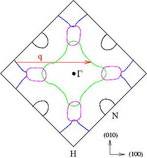
Many low-dimensional solids have anisotropic Fermi surfaces that have prominent nesting vectors. Well-known examples include layered materials like NbSe3, TaSe2 and K0.3MoO3 (a Chevrel phase) and quasi-1D organic conductors like TMTSF or TTF-TCNQ. CDWs are also common at the surface of solids where they are more commonly called surface reconstructions or even dimerization. Surfaces so often support CDWs because they can be described by two-dimensional Fermi surfaces like those of layered materials. Chains of Au and In on semiconducting substrates have been shown to exhibit CDWs. More recently, monatomic chains of Co on a metallic substrate were experimentally shown to exhibit a CDW instability and was attributed to ferromagnetic correlations.
The most intriguing properties of density waves are their dynamics. Under an appropriate electric field or magnetic field, a density wave will "slide" in the direction indicated by the field due to the electrostatic or magnetostatic force. Typically the sliding will not begin until a "depinning" threshold field is exceeded where the wave can escape from a potential well caused by a defect. The hysteretic motion of density waves is therefore not unlike that of dislocations or magnetic domains. The current-voltage curve of a CDW solid therefore shows a very high electrical resistance up to the depinning voltage, above which it shows a nearly ohmic behavior. Under the depinning voltage (which depends on the purity of the material), the crystal is an insulator.
