 | ||
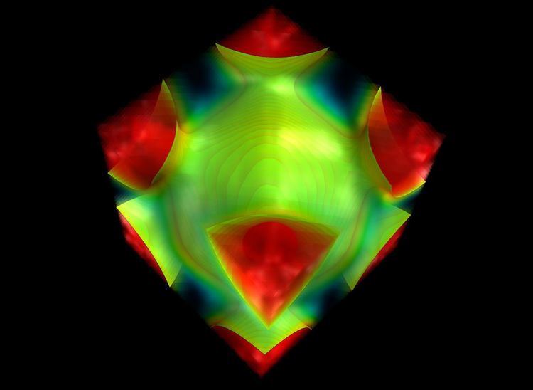
In condensed matter physics, the Fermi surface is an abstract boundary in reciprocal space useful for predicting the thermal, electrical, magnetic, and optical properties of metals, semimetals, and doped semiconductors. The shape of the Fermi surface is derived from the periodicity and symmetry of the crystalline lattice and from the occupation of electronic energy bands. The existence of a Fermi surface is a direct consequence of the Pauli exclusion principle, which allows a maximum of one electron per quantum state.
Contents
Theory
Consider a spinless ideal Fermi gas of
where,
Suppose we consider the limit
By the Pauli exclusion principle, no two fermions can be in the same state. Therefore, in the state of lowest energy, the particles fill up all energy levels below
In momentum space, these particles fill up a sphere of radius
The linear response of a metal to an electric, magnetic or thermal gradient is determined by the shape of the Fermi surface, because currents are due to changes in the occupancy of states near the Fermi energy. Free-electron Fermi surfaces are spheres of radius
determined by the valence electron concentration where
Materials with complex crystal structures can have quite intricate Fermi surfaces. The figure illustrates the anisotropic Fermi surface of graphite, which has both electron and hole pockets in its Fermi surface due to multiple bands crossing the Fermi energy along the
The state occupancy of fermions like electrons is governed by Fermi–Dirac statistics so at finite temperatures the Fermi surface is accordingly broadened. In principle all fermion energy level populations are bound by a Fermi surface although the term is not generally used outside of condensed-matter physics.
Experimental determination
Electronic Fermi surfaces have been measured through observation of the oscillation of transport properties in magnetic fields
Observation of the dHvA and SdH oscillations requires magnetic fields large enough that the circumference of the cyclotron orbit is smaller than a mean free path. Therefore, dHvA and SdH experiments are usually performed at high-field facilities like the High Field Magnet Laboratory in Netherlands, Grenoble High Magnetic Field Laboratory in France, the Tsukuba Magnet Laboratory in Japan or the National High Magnetic Field Laboratory in the United States.
The most direct experimental technique to resolve the electronic structure of crystals in the momentum-energy space (see reciprocal lattice), and, consequently, the Fermi surface, is the angle resolved photoemission spectroscopy (ARPES). An example of the Fermi surface of superconducting cuprates measured by ARPES is shown in the figure.
With positron annihilation it is also possible to determine the Fermi surface as the annihilation process conserves the momentum of the initial particle. Since a positron in a solid will thermalize prior to annihilation, the annihilation radiation carries the information about the electron momentum. The corresponding experimental technique is called angular correlation of electron positron annihilation radiation (ACAR) as it measures the angular deviation from 7002180000000000000♠180 degree of both annihilation quanta. In this way it is possible to probe the electron momentum density of a solid and determine the Fermi surface. Furthermore, using spin polarized positrons, the momentum distribution for the two spin states in magnetized materials can be obtained. ACAR has many advantages and disadvantages compared to other experimental techniques: It does not rely on UHV conditions, cryogenic temperatures, high magnetic fields or fully ordered alloys. However, ACAR needs samples with a low vacancy concentration as they act as effective traps for positrons. In this way, the first determination of a smeared Fermi surface in a 30% alloy was obtained in 1978.
