
 | ||
Tutorial video on piezophototronics by prof zhong lin wang
Piezo-phototronic effect is a three way coupling effect of piezoelectric, semiconductor and photonic properties in non-central symmetric semiconductor materials, using the piezoelectric potential (piezopotential) that is generated by applying a strain to a semiconductor with piezoelectricity to control the carrier generation, transport, separation and/or recombination at metal-semiconductor junction or p-n junction for improving the performance of optoelectronic devices, such as photodetector, solar cell and light-emitting diode. Prof. Zhong Lin Wang at Georgia Institute of Technology proposed the fundamental principle of this effect in 2010.
Contents
Mechanism
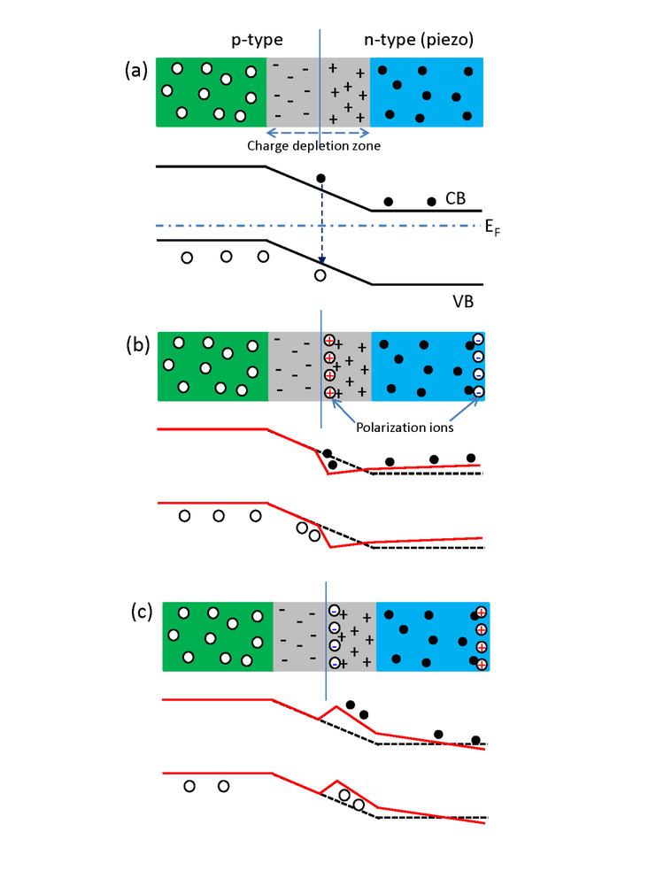
When a p-type semiconductor and a n-type semiconductor form a junction, the holes in the p-type side and the electrons in the n-type side tend to redistribute around the interface area to balance the local electric field, which results in a charge depletion layer. The diffusion and recombination of the electrons and holes in the junction region is close related to the optoelectronic properties of the device, which is greatly affected by the local electric field distribution. The existence of the piezo-charges at the interface introduces three effects: a shift in local electronic band structure due to the introduced local potential, a tilt of the electronic band structure over the junction region for the polarization existing in the piezoelectric semiconductor, and a change in the charge depletion layer due to the redistribution of the local charge carriers to balance the local piezo-charges. The positive piezoelectric charges at the junction lower the energy band and the negative piezoelectric charges raise the energy band in n-type semiconductor region near the junction region. A modification in the local band by piezopotential may be effective for trapping charges so that the electron-hole recombination rate can be largely enhanced, which is very beneficial for improving the efficiency of a light-emitting diode. Furthermore, the inclined band tends to change the mobility of the carriers moving toward the junction. The materials for piezo-phototronics should have three basic properties: piezoelectricity, semiconductor property, and photon excitation property [5]. Typical materials are the wurtzite structures, such as ZnO, GaN and InN. the three-way coupling among piezoelectricity, photoexcitation and semiconductor properties, which is the basis of piezotronics (piezoelectricity-semiconductor coupling), piezophotonics (piezoelectric-photon excitation coupling), optoelectronics, and piezo-phototronics piezoelectricity-semiconductor-photoexcitation). The core of these coupling relies on the piezopotential created by the piezoelectric materials.