
 | ||
Piezotronics effect is using the piezoelectric potential (piezopotential) created in materials with piezoelectricity as a “gate” voltage to tune/control the charge carrier transport properties for fabricating new devices. Neil A Downie showed how simple it was to build simple demonstrations on a macro-scale using a sandwich of piezoelectric material and carbon piezoresistive material to make an FET-like amplifying device and put it in a book of science projects for students in 2006. The fundamental principle of piezotronics was introduced by Prof. Zhong Lin Wang at Georgia Institute of Technology in 2007 . A series of electronic devices have been demonstrated based on this effect, including piezopotential gated field-effect transistor, piezopotential gated diode, strain sensors, force/flow sensors, hybrid field-effect transistor, piezotronic logic gates, electromechanical memories, etc. Piezotronic devices are regarded as a new semiconductor-device category. Piezotronics is likely to have important applications in sensor, human-silicon technology interfacing, MEMS, nanorobotics and active flexible electronics.
Mechanism
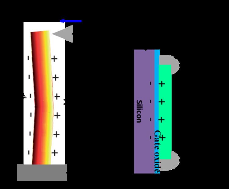
Due to the non-central symmetry in materials such as the wurtzite structured ZnO, GaN and InN, a piezopotential is created in the crystal by applying a stress. Owing to the simultaneous possession of piezoelectricity and semiconductor properties, the piezopotential created in the crystal has a strong effect on the carrier transport process. Generally, the construction of the basic piezotronic devices can be divided into two categories. Here we use the nanowires as the example. The first kind is that the piezoelectric nanowire was put on a flexible substrate with two ends fixed by the electrodes. In this case, when the substrate is bended, the nanowire will be purely stretched or compressed. Piezopotential will be introduced along its axis. It will modify the electric field or the Schottky barrier (SB) height at the contact area. The induced positive piezopotential at one end will reduce the SB height, while the negative piezopotential at the other end will increase it. Thus the electric transport properties will be changed. The second kind of the piezotronic device is that one end of the nanowire is fixed with electrode, while the other end is free. In this case, when a force is applied at the free end of the nanowire to bend it, the piezopotential distribution will be perpendicular to the axis of the nanowire. The introduced piezoelectric field is perpendicular to electron transport direction, just like applying a gate voltage in the traditional field-effect transistor. Thus the electron transport properties will also be changed. The materials for piezotronics should be piezoelectric semiconductors, such as ZnO, GaN and InN. Three-way coupling among piezoelectricity, photoexcitation and semiconductor is the basis of piezotronics (piezoelectricity-semiconductor coupling), piezophotonics (piezoelectric-photon excitation coupling), optoelectronics, and piezophototronics (piezoelectricity-semiconductor-photoexcitation). The core of these coupling relies on the piezopotential created by the piezoelectric materials.