
FSB speeds 66 MHz to 100 MHz | Max. CPU clock rate 233 MHz to 450 MHz Min. feature size 0.35 µm to 0.18 µm | |
 | ||
Produced From mid-1997 to early 1999 | ||
The Pentium II brand refers to Intel's sixth-generation microarchitecture ("P6") and x86-compatible microprocessors introduced on May 7, 1997. Containing 7.5 million transistors (27.4 million in the case of the mobile Dixon with 256 KB L2 cache), the Pentium II featured an improved version of the first P6-generation core of the Pentium Pro, which contained 5.5 million transistors. However, its L2 cache subsystem was a downgrade when compared to Pentium Pros. In early 1999, the Pentium II was superseded by the almost identical Pentium III, which basically only added SSE instructions to the CPU.
Contents
- Overview
- Klamath
- Deschutes
- Pentium II OverDrive
- Tonga
- Dixon
- Klamath 80522
- Deschutes 80523
- Deschutes Pentium II Overdrive
- Tonga 80523
- Dixon 80524
- References
In 1998, Intel stratified the Pentium II family by releasing the Pentium II-based Celeron line of processors for low-end workstations and the Pentium II Xeon line for servers and high-end workstations. The Celeron was characterized by a reduced or omitted (in some cases present but disabled) on-die full-speed L2 cache and a 66 MT/s FSB. The Xeon was characterized by a range of full-speed L2 cache (from 512 KB to 2048 KB), a 100 MT/s FSB, a different physical interface (Slot 2), and support for symmetric multiprocessing.
Overview
The Pentium II microprocessor was largely based upon the microarchitecture of its predecessor, the Pentium Pro, but with some significant improvements.
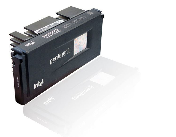
Unlike previous Pentium and Pentium Pro processors, the Pentium II CPU was packaged in a slot-based module rather than a CPU socket. The processor and associated components were carried on a daughterboard similar to a typical expansion board within a plastic cartridge. A fixed or removable heatsink was carried on one side, sometimes using its own fan.
This larger package was a compromise allowing Intel to separate the secondary cache from the processor while still keeping it on a closely coupled back-side bus. The L2 cache ran at half the processor's clock frequency, unlike the Pentium Pro, whose off die L2 cache ran at the same frequency as the processor. However, the smallest cache size was increased to 512 KB from the 256 KB on the Pentium Pro. Off-package cache solved the Pentium Pro's low yields, allowing Intel to introduce the Pentium II at a mainstream price level. This arrangement also allowed Intel to easily vary the amount of L2 cache, thus making it possible to target different market segments with cheaper or more expensive processors and accompanying performance levels.
Intel improved 16-bit code execution performance on the Pentium II, an area in which the Pentium Pro was at a notable handicap; this was achieved with the addition of segment register caches. Most consumer software of the day was still using at least some 16-bit code, because of a variety of factors. The Pentium II featured 32 KB of L1 cache, double that of the Pentium Pro, as well as deeper write buffers for a slight L1 performance increase. The Pentium II was also the first P6-based CPU to implement the Intel MMX integer SIMD instruction set which had already been introduced on the Pentium MMX.
The Pentium II was basically a more consumer-oriented version of the Pentium Pro. It was cheaper to manufacture because of the separate, slower L2 cache memory. The improved 16-bit performance and MMX support made it a better choice for consumer-level operating systems, such as Windows 9x, and multimedia applications. Combined with the larger L1 cache and improved 16-bit performance, the slower and cheaper L2 cache's performance impact was reduced. General processor performance was increased while costs were cut.
All Klamath and some early Deschutes Pentium IIs use a combined L2 cache controller / tag RAM chip that only allows for 512 MB to be cached; while more RAM could be installed in theory, this would result in very slow performance. While this limit was practically irrelevant for the average home user at the time, it was a concern for some workstation or server users. Presumably, Intel put this limitation deliberately in place to distinguish the Pentium II from the more higher end Pentium Pro line, which has a full 4 GB cacheable area. The '82459AD' revision of the chip on some 333 MHz and all 350 MHz and faster Pentium IIs lifted this restriction and also offered a full 4 GB cacheable area.
Klamath
The original Klamath Pentium II microprocessor (Intel product code 80522) ran at 233, 266, and 300 MHz and were produced in a 0.35 µm process. The 300 MHz version, however, only became available in quantities later in 1997. These CPUs had a 66 MHz front side bus and were initially used on motherboards equipped with the aging Intel 440FX Natoma chipset designed for the Pentium Pro. Pentium II-based systems using the Intel 440LX Balboa chipset were the first to utilize the new generation RAM-standard, SDRAM (which replaced EDO RAM), and the AGP graphics bus.
On July 14, 1997, Intel announced a version of the Pentium II Klamath with 2x 72-bit ECC L2 cache for entry-level servers, as opposed to the 2x 64-bit non-ECC L2 cache on regular models. This means that identically clocked Pentium IIs can have a very slight performance difference. The variant can be determined through the CPU part number.
In Intel's "Family/Model/Stepping" scheme, Klamath CPUs are family 6, model 3.
Deschutes
The Deschutes core Pentium II (80523), which debuted at 333 MHz in January 1998, was produced with a 0.25 µm process and has a significantly lower power draw. The die size is 113 mm2. The 333 MHz variant was the final Pentium CPU that used the older 66 MHz front side bus; all subsequent Deschutes-core models used a 100 MHz FSB. Later in 1998, Pentium IIs running at 266, 300, 350, 400, and 450 MHz were also released. The Deschutes core introduced FXSAVE and FXRSTOR instructions for fast FPU context save and restore. Towards the end of its design life, Deschutes chips capable of 500 MHz within Intel cooling and design specifications were produced. However, these were not marketed. Rather than destroy already multiplier-locked units, those Deschutes units that had been tested and locked with a multiplier of 5 were sold as being 333 MHz. This was accomplished by disabling the 100 MHz bus option. Overclockers, upon learning of this, purchased the units in question and ran them well over 500 MHz; most notably, when overclocking, the final batch of "333 MHz" CPUs were capable of speeds much higher than CPUs sold at 350, 400, or 450 MHz.
Concurrent with the release of Deschutes cores supporting a 100 MHz front side bus was Intel's release of the 440BX Seattle chipset and its derivatives, the 440MX, 450NX, and 440ZX chipsets. The 100 MHz front side bus speed resulted in solid performance improvements for the Pentium II lineup. Pentium II chips starting with 350 MHz were released in both SECC and SECC2 form factors. Late Pentium IIs also marked the switch to flip-chip based packaging with direct heatsink contact to the die.
While Klamath features 4 cache chips and simulates dual-porting through interleaving (2x 64-bit) for a slight performance improvement on concurrent accesses, Deschutes only sports 2 cache chips and offers slightly lower L2 cache performance at the same clockspeed. Furthermore, Deschutes always features ECC-enabled L2 cache.
The Pentium II Xeon was a high-end version of Deschutes core intended for use on workstations and servers. Principally, it used a different type of slot (Slot 2), case, board design, and more expensive full-speed custom L2 cache, which was off-die. Versions were produced with 512 KB, 1 MB or 2 MB L2 caches by varying the number of 512 KB chips incorporated on the board.
In Intel's "Family/Model/Stepping" scheme, Deschutes CPUs are family 6, model 5 and have the part number 80523.
Pentium II OverDrive
In 1998, the 0.25 μm Deschutes core was utilized in the creation of the Pentium II Overdrive processor, which was aimed at allowing corporate Pentium Pro users to upgrade their aging servers. Combining the Deschutes core in a flip-chip package with a 512 KB full-speed L2 cache chip from the Pentium II Xeon into a Socket 8-compatible module resulted in a 300 or 333 MHz processor that could run on a 60 or 66 MHz front side bus. This combination brought together some of the more attractive aspects of the Pentium II and the Pentium II Xeon: MMX support/improved 16-bit performance and full-speed L2 cache, respectively. The later "Dixon" mobile Pentium II would emulate this combination with 256 KB of full-speed cache.
In Intel's "Family/Model/Stepping" scheme, the Pentium II OverDrive CPU identifies itself as family 6, model 3, though this is misleading, as it is not based on the family 6/model 3 Klamath core. As noted in the Pentium II Processor update documentation from Intel, "Please note that although this processor has a CPUID of 163xh, it uses a Pentium II processor CPUID 065xh processor core."
Tonga
The 0.25 μm Tonga core was the first mobile Pentium II and had all of the features of the desktop models.
In Intel's "Family/Model/Stepping" scheme, Tonga CPUs are family 6, model 5.
Dixon
Later, in 1999, the 0.25; 0.18 (400 MHz) μm Dixon core with 256 KB of on-die full speed cache was produced for the mobile market. Reviews showed that the Dixon core was the fastest type of Pentium II produced.
In Intel's "Family/Model/Stepping" scheme, Dixon CPUs are family 6, model 6 and their Intel product code is 80524. These identifiers are shared with the Mendocino Celeron processors.
Klamath (80522)
Deschutes (80523)
Deschutes (Pentium II Overdrive)
Tonga (80523)
Mobile Pentium II
Dixon (80524)
Mobile Pentium II PE ("Performance Enhanced")