
Type Slot FSB protocol GTL+ | Contacts 242 Voltage range 1.3 to 3.50 V | |
 | ||
Chip form factors Single Edge Contact Cartridge (Pentium II)Single Edge Contact Cartridge 2 (Pentium II, Pentium III)Single Edge Processor Package (Celeron) FSB frequency 66, 100, and (on third-party chipsets) 133 MHz | ||
Slot 1 refers to the physical and electrical specification for the connector used by some of Intel's microprocessors, including the Pentium Pro, Celeron, Pentium II and the Pentium III. Both single and dual processor configurations were implemented.
Contents
General
With the introduction of the Pentium II CPU, the need for greater access for testing had made the transition from socket to slot necessary. Previously with the Pentium Pro, Intel had combined processor and cache dies in the same Socket 8 package. These were connected by a full-speed bus, resulting in significant performance benefits. Unfortunately, this method required that the two components be bonded together early in the production process, before testing was possible. As a result, a single, tiny flaw in either die made it necessary to discard the entire assembly, causing low production yield and high cost.
Intel subsequently designed a circuit board where the CPU and cache remained closely integrated, but were mounted on a printed circuit board, called a Single-Edged Contact Cartridge (SECC). The CPU and cache could be tested separately, before final assembly into a package, reducing cost and making the CPU more attractive to markets other than that of high-end servers. These cards could also be easily plugged into a Slot 1, thereby eliminating the chance for pins of a typical CPU to be bent or broken when installing in a socket.
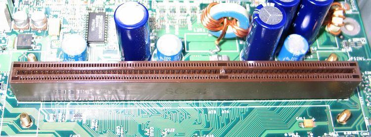
The form factor used for Slot 1 was a 5-inch-long, 242-contact edge connector named SC242. To prevent the cartridge from being inserted the wrong way, the slot was keyed to allow installation in only one direction. The SC242 was later used for AMD's Slot A as well, and while the two slots were identical mechanically, they were electrically incompatible. To discourage Slot A users from trying to install a Slot 1 CPU, the connector was rotated 180 degrees on Slot A motherboards.
With the new Slot 1, Intel added support for symmetric multiprocessing (SMP). A maximum of two Pentium II or Pentium III CPUs can be used in a dual slot motherboard. The Celeron does not have official SMP support.
There are also converter cards, known as Slotkets, which hold a Socket 8 so that a Pentium Pro CPU can be used with Slot 1 motherboards. These specific converters, however, are rare. Another kind of slotket allows using a Socket 370 CPU in a Slot 1. Many of these latter devices are equipped with own voltage regulator modules, in order to supply the new CPU with a lower core voltage, which the motherboard would not otherwise allow.
Form Factors
The Single Edge Contact Cartridge, or "SECC", was used at the beginning of the Slot 1-era for Pentium II CPUs. Inside the cartridge, the CPU itself is enclosed in a hybrid plastic and metal case. The back of the housing is plastic and has several markings on it: the name, "Pentium II"; the Intel logo; a hologram; and the model number. The front consists of a black anodized aluminum plate, which is used to hold the CPU cooler. The SECC form is very solid, because the CPU itself is resting safely inside the case. As compared to socket-based CPUs, there are no pins that can be bent, and the CPU is less likely to be damaged by improper installation of a cooler.
Following SECC, the SEPP-form (Single Edge Processor Package) appeared on the market. It was designed for lower-priced Celeron CPUs. This form lacks a case entirely, consisting solely of the printed-circuit board holding the components.
A form factor called SECC2 was used for late Pentium II and Pentium III CPUs for Slot 1, which was created to accommodate the switch to flip chip packaging. Only the front plate was carried over, the coolers were now mounted straight to the PCB and exposed CPU die and are, as such, incompatible with SECC cartridges.
History
Historically, there are three platforms for the Intel P6-CPUs: Socket 8, Slot 1 and Socket 370.
Slot 1 is a successor to Socket 8. While the Socket 8 CPUs (Pentium Pro) directly had the L2-cache embedded into the CPU, it is located (outside of the core) on a circuit board shared with the core itself. The exception is later Slot 1 CPUs with the Coppermine core which have the L2-Cache embedded into the die.
In the beginning of 2000, while the Pentium-III-CPUs with FC-PGA-housing appeared, Slot 1 was slowly succeeded by Socket 370, after Intel had already offered Socket 370 and Slot 1 at the same time since the beginning of 1999. Socket 370 was initially made for the low-cost Celeron processors, while Slot 1 was thought of as a platform for the expensive Pentium II and early Pentium III models. Cache and core were both embedded into the die.
Slot 1 also obsoleted the old Socket 7, at least regarding Intel, as the standard platform for the home-user. After abandoning the Intel P5 Pentium MMX CPU, Intel completely left the Socket 7 market to the manufacturers AMD, Cyrix and IDT.