
 | ||
Within materials science, the optical properties of carbon nanotubes refer specifically to the absorption, photoluminescence (fluorescence), and Raman spectroscopy of carbon nanotubes. Spectroscopic methods offer the possibility of quick and non-destructive characterization of relatively large amounts of carbon nanotubes. There is a strong demand for such characterization from the industrial point of view: numerous parameters of the nanotube synthesis can be changed, intentionally or unintentionally, to alter the nanotube quality. As shown below, optical absorption, photoluminescence and Raman spectroscopies allow quick and reliable characterization of this "nanotube quality" in terms of non-tubular carbon content, structure (chirality) of the produced nanotubes, and structural defects. Those features determine nearly any other properties such as optical, mechanical, and electrical properties.
Contents
- Terminology
- Electronic structure of carbon nanotube
- Van Hove singularities
- Kataura plot
- Optical absorption
- Carbon nanotubes as a black body
- Photoluminescence Fluorescence
- Salient properties
- Applications
- Sensitization
- Cathodoluminescence
- Electroluminescence
- Raman scattering
- Radial breathing mode
- Bundling mode
- G mode
- D mode
- Anti Stokes scattering
- Rayleigh scattering
- References
Carbon nanotubes are unique "one-dimensional systems" which can be envisioned as rolled single sheets of graphite (or more precisely graphene). This rolling can be done at different angles and curvatures resulting in different nanotube properties. The diameter typically varies in the range 0.4–40 nm (i.e. "only" ~100 times), but the length can vary ~10,000 times, reaching 55.5 cm. The nanotube aspect ratio, or the length-to-diameter ratio, can be as high as 132,000,000:1, which is unequalled by any other material. Consequently, all the properties of the carbon nanotubes relative to those of typical semiconductors are extremely anisotropic (directionally dependent) and tunable.
Whereas mechanical, electrical and electrochemical (supercapacitor) properties of the carbon nanotubes are well established and have immediate applications, the practical use of optical properties is yet unclear. The aforementioned tunability of properties is potentially useful in optics and photonics. In particular, light-emitting diodes (LEDs) and photo-detectors based on a single nanotube have been produced in the lab. Their unique feature is not the efficiency, which is yet relatively low, but the narrow selectivity in the wavelength of emission and detection of light and the possibility of its fine tuning through the nanotube structure. In addition, bolometer and optoelectronic memory devices have been realised on ensembles of single-walled carbon nanotubes.
Terminology
This article uses the following abbreviations:
However, C is often omitted in scientific literature, so NT, SWNT and MWNT are more commonly used. Also, "wall" is often exchanged with "walled".
Electronic structure of carbon nanotube
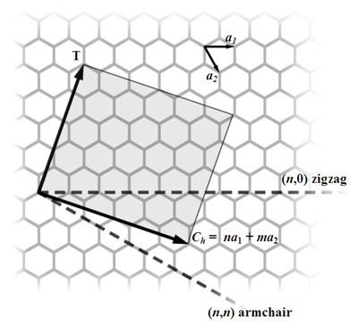
A single-wall carbon nanotube can be imagined as graphene sheet rolled at a certain "chiral" angle with respect to a plane perpendicular to the tube's long axis. Consequently, SWCNT can be defined by its diameter and chiral angle. The chiral angle can range from 0 to 30 degrees.
However, more conveniently, a pair of indices (n, m) is used instead. The indices refer to equally long unit vectors at 60° angles to each other across a single 6-member carbon ring. Taking the origin as carbon number 1, the a1 unit vector may be considered the line drawn from carbon 1 to carbon 3, and the a2 unit vector is then the line drawn from carbon 1 to carbon 5. (See the upper right corner of the diagram at right.) To visualize a CNT with indices (n, m), draw n a1 unit vectors across the graphene sheet, then draw m a2 unit vectors at a 60° angle to the a1 vectors, then add the vectors together. The line representing the sum of the vectors will define the circumference of the CNT along the plane perpendicular to its long axis, connecting one end to the other. In the diagram at right, Ch is a (4, 2) vector: the sum of 4 unit vectors from the origin directly to the right, then 2 unit vectors at a 60° angle down and to the right.
Tubes having n = m (chiral angle = 30°) are called "armchair" and those with m = 0 (chiral angle = 0°) "zigzag". Those indices uniquely determine whether CNT is a metal, semimetal or semiconductor, as well as its band gap: when |m – n| = 3k (k is integer), the tube is metallic; but if |m – n| = 3k ± 1, the tube is semiconducting. The nanotube diameter d is related to m and n as
In this equation, a = 0.246 nm is the magnitude of either unit vector a1 or a2.
The situation in multi-wall CNTs is complicated as their properties are determined by contribution of all individual shells; those shells have different structures, and, because of the synthesis, are usually more defective than SWCNTs. Therefore, optical properties of MWCNTs will not be considered here.
Van Hove singularities
Optical properties of carbon nanotubes derive from electronic transitions within one-dimensional density of states (DOS). A typical feature of one-dimensional crystals is that their DOS is not a continuous function of energy, but it descends gradually and then increases in a discontinuous spike. In contrast, three-dimensional materials have continuous DOS. The sharp peaks found in one-dimensional materials are called Van Hove singularities.
Van Hove singularities result in the following remarkable optical properties of carbon nanotubes:
Kataura plot
The band structure of carbon nanotubes having certain (n, m) indexes can be easily calculated. A theoretical graph based on this calculations was designed in 1999 by Hiromichi Kataura to rationalize experimental findings. A Kataura plot relates the nanotube diameter and its bandgap energies for all nanotubes in a diameter range. The oscillating shape of every branch of the Kataura plot reflects the intrinsic strong dependence of the SWCNT properties on the (n, m) index rather than on its diameter. For example, (10, 1) and (8, 3) tubes have almost the same diameter, but very different properties: the former is a metal, but the latter is a semiconductor.
Optical absorption
Optical absorption in carbon nanotubes differs from absorption in conventional 3D materials by presence of sharp peaks (1D nanotubes) instead of an absorption threshold followed by an absorption increase (most 3D solids). Absorption in nanotubes originates from electronic transitions from the v2 to c2 (energy E22) or v1 to c1 (E11) levels, etc. The transitions are relatively sharp and can be used to identify nanotube types. Note that the sharpness deteriorates with increasing energy, and that many nanotubes have very similar E22 or E11 energies, and thus significant overlap occurs in absorption spectra. This overlap is avoided in photoluminescence mapping measurements (see below), which instead of a combination of overlapped transitions identifies individual (E22, E11) pairs.
Interactions between nanotubes, such as bundling, broaden optical lines. While bundling strongly affects photoluminescence, it has much weaker effect on optical absorption and Raman scattering. Consequently, sample preparation for the latter two techniques is relatively simple.
Optical absorption is routinely used to quantify quality of the carbon nanotube powders.
The spectrum is analyzed in terms of intensities of nanotube-related peaks, background and pi-carbon peak; the latter two mostly originate from non-nanotube carbon in contaminated samples. However, it has been recently shown that by aggregating nearly single chirality semiconducting nanotubes into closely packed Van der Waals bundles the absorption background can be attributed to free carrier transition originating from intertube charge transfer.
Carbon nanotubes as a black body
An ideal black body should have emissivity or absorbance of 1.0, which is difficult to attain in practice, especially in a wide spectral range. Vertically aligned "forests" of single-wall carbon nanotubes can have absorbances of 0.98–0.99 from the far-ultraviolet (200 nm) to far-infrared (200 μm) wavelengths.
These SWNT forests (buckypaper) were grown by the super-growth CVD method to about 10 μm height. Two factors could contribute to strong light absorption by these structures: (i) a distribution of CNT chiralities resulted in various bandgaps for individual CNTs. Thus a compound material was formed with broadband absorption. (ii) Light might be trapped in those forests due to multiple reflections.
Photoluminescence (Fluorescence)
Semiconducting single-walled carbon nanotubes emit near-infrared light upon photoexcitation, described interchangeably as fluorescence or photoluminescence (PL). The excitation of PL usually occurs as follows: an electron in a nanotube absorbs excitation light via S22 transition, creating an electron-hole pair (exciton). Both electron and hole rapidly relax (via phonon-assisted processes) from c2 to c1 and from v2 to v1 states, respectively. Then they recombine through a c1 − v1 transition resulting in light emission.
No excitonic luminescence can be produced in metallic tubes. Their electrons can be excited, thus resulting in optical absorption, but the holes are immediately filled by other electrons out of the many available in the metal. Therefore, no excitons are produced.
Salient properties
Applications
Sensitization
Optical properties, including the PL efficiency, can be modified by encapsulating organic dyes (carotene, lycopene, etc.) inside the tubes. Efficient energy transfer occurs between the encapsulated dye and nanotube — light is efficiently absorbed by the dye and without significant loss is transferred to the SWCNT. Thus potentially, optical properties of a carbon nanotube can be controlled by encapsulating certain molecule inside it. Besides, encapsulation allows isolation and characterization of organic molecules which are unstable under ambient conditions. For example, Raman spectra are extremely difficult to measure from dyes because of their strong PL (efficiency close to 100%). However, encapsulation of dye molecules inside SWCNTs completely quenches dye PL, thus allowing measurement and analysis of their Raman spectra.
Cathodoluminescence
Cathodoluminescence (CL) — light emission excited by electron beam — is a process commonly observed in TV screens. An electron beam can be finely focused and scanned across the studied material. This technique is widely used to study defects in semiconductors and nanostructures with nanometer-scale spatial resolution. It would be beneficial to apply this technique to carbon nanotubes. However, no reliable CL, i.e. sharp peaks assignable to certain (n, m) indices, has been detected from carbon nanotubes yet.
Electroluminescence
If appropriate electrical contacts are attached to a nanotube, electron-hole pairs (excitons) can be generated by injecting electrons and holes from the contacts. Subsequent exciton recombination results in electroluminescence (EL). Electroluminescent devices have been produced from single nanotubes and their macroscopic assemblies. Recombination appears to proceed via triplet-triplet annihilation giving distinct peaks corresponding to E11 and E22 transitions.
Raman scattering
Raman spectroscopy has good spatial resolution (~0.5 micrometers) and sensitivity (single nanotubes); it requires only minimal sample preparation and is rather informative. Consequently, Raman spectroscopy is probably the most popular technique of carbon nanotube characterization. Raman scattering in SWCNTs is resonant, i.e., only those tubes are probed which have one of the bandgaps equal to the exciting laser energy. Several scattering modes dominate the SWCNT spectrum, as discussed below.
Similar to photoluminescence mapping, the energy of the excitation light can be scanned in Raman measurements, thus producing Raman maps. Those maps also contain oval-shaped features uniquely identifying (n, m) indices. Contrary to PL, Raman mapping detects not only semiconducting but also metallic tubes, and it is less sensitive to nanotube bundling than PL. However, requirement of a tunable laser and a dedicated spectrometer is a strong technical impediment.
Radial breathing mode
Radial breathing mode (RBM) corresponds to radial expansion-contraction of the nanotube. Therefore, its frequency νRBM (in cm−1) depends on the nanotube diameter d as, νRBM= A/d + B (where A and B are constants dependent on the environment in which the nanotube is present. For example, B=0 for individual nanotubes.) (in nanometers) and can be estimated as νRBM = 234/d + 10 for SWNT or νRBM = 248/d for DWNT, which is very useful in deducing the CNT diameter from the RBM position. Typical RBM range is 100–350 cm−1. If RBM intensity is particularly strong, its weak second overtone can be observed at double frequency.
Bundling mode
The bundling mode is a special form of RBM supposedly originating from collective vibration in a bundle of SWCNTs.
G mode
Another very important mode is the G mode (G from graphite). This mode corresponds to planar vibrations of carbon atoms and is present in most graphite-like materials. G band in SWCNT is shifted to lower frequencies relative to graphite (1580 cm−1) and is split into several peaks. The splitting pattern and intensity depend on the tube structure and excitation energy; they can be used, though with much lower accuracy compared to RBM mode, to estimate the tube diameter and whether the tube is metallic or semiconducting.
D mode
D mode is present in all graphite-like carbons and originates from structural defects. Therefore, the ratio of the G/D modes is conventionally used to quantify the structural quality of carbon nanotubes. High-quality nanotubes have this ratio significantly higher than 100. At a lower functionalisation of the nanotube, the G/D ratio remains almost unchanged. This ratio gives an idea of the functionalisation of a nanotube.
G' mode
The name of this mode is misleading: it is given because in graphite, this mode is usually the second strongest after the G mode. However, it is actually the second overtone of the defect-induced D mode (and thus should logically be named D'). Its intensity is stronger than that of the D mode due to different selection rules. In particular, D mode is forbidden in the ideal nanotube and requires a structural defect, providing a phonon of certain angular momentum, to be induced. In contrast, G' mode involves a "self-annihilating" pair of phonons and thus does not require defects. The spectral position of G' mode depends on diameter, so it can be used roughly to estimate the SWCNT diameter. In particular, G' mode is a doublet in double-wall carbon nanotubes, but the doublet is often unresolved due to line broadening.
Other overtones, such as a combination of RBM+G mode at ~1750 cm−1, are frequently seen in CNT Raman spectra. However, they are less important and are not considered here.
Anti-Stokes scattering
All the above Raman modes can be observed both as Stokes and anti-Stokes scattering. As mentioned above, Raman scattering from CNTs is resonant in nature, i.e. only tubes whose band gap energy is similar to the laser energy are excited. The difference between those two energies, and thus the band gap of individual tubes, can be estimated from the intensity ratio of the Stokes/anti-Stokes lines. This estimate however relies on the temperature factor (Boltzmann factor), which is often miscalculated – a focused laser beam is used in the measurement, which can locally heat the nanotubes without changing the overall temperature of the studied sample.
Rayleigh scattering
Carbon nanotubes have very large aspect ratio, i.e., their length is much larger than their diameter. Consequently, as expected from the classical electromagnetic theory, elastic light scattering (or Rayleigh scattering) by straight CNTs has anisotropic angular dependence, and from its spectrum, the band gaps of individual nanotubes can be deduced.
Another manifestation of Rayleigh scattering is the "antenna effect", an array of nanotubes standing on a substrate has specific angular and spectral distributions of reflected light, and both those distributions depend on the nanotube length.