
 | ||
The nanomesh is a new inorganic nanostructured two-dimensional material, similar to graphene. It was discovered in 2003 at the University of Zurich, Switzerland .
Contents
- Nanomesh scarf tutorial zbrush
- Structure
- Properties
- Preparation and analysis
- Other forms
- Other links
- References
It consists of a single layer of boron (B) and nitrogen (N) atoms, which forms by self-assembly a highly regular mesh after high-temperature exposure of a clean rhodium or ruthenium surface to borazine under ultra-high vacuum.
The nanomesh looks like an assembly of hexagonal pores (see right image) at the nanometer (nm) scale. The distance between 2 pore centers is only of 3.2 nm, whereas each pore has a diameter of about 2 nm and is 0.05 nm deep. The lowest regions bind strongly to the underlying metal, while the wires (highest regions) are only bound to the surface through strong cohesive forces within the layer itself.
The boron nitride nanomesh is not only stable under vacuum, air and some liquids, but also up to temperatures of 796oC (1070 K). In addition it shows the extraordinary ability to trap molecules and metallic clusters, which have similar sizes to the nanomesh pores, forming a well-ordered array. These characteristics promise interesting applications of the nanomesh in areas like nanocatalysis, surface functionalisation, spintronics, quantum computing and data storage media like hard drives.
Nanomesh scarf tutorial zbrush
Structure
h-BN nanomesh is a single sheet of hexagonal boron nitride, which forms on substrates like rhodium Rh(111) or ruthenium Ru(0001) crystals by a self-assembly process.
The unit cell of the h-BN nanomesh consists of 13x13 BN or 12x12 Rh atoms with a lattice constant of 3.2 nm. In a cross-section it means that 13 boron or nitrogen atoms are sitting on 12 rhodium atoms. This implies a modification of the relative positions of each BN towards the substrate atoms within a unit cell, where some bonds are more attractive or repulsive than other (site selective bonding), what induces the corrugation of the nanomesh (see right image with pores and wires).
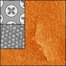
The nanomesh corrugation amplitude of 0.05 nm causes a strong effect on the electronic structure, where two distinct BN regions are observed. They are easily recognized in the lower right image, which is a scanning tunneling microscopy (STM) measurement, as well as in the lower left image representing a theoretical calculation of the same area. A strongly bounded region assigned to the pores is visible in blue in the left image below (center of bright rings in the right image) and a weakly bound region assigned to the wires appears yellow-red in the left image below (area in-between rings in the right image).
See for more details.
Properties
The nanomesh is stable under a wide range of environments like air, water and electrolytes among others. It is also temperature resistant since it doesn't decompose up to 1275K under vacuum. In addition to these exceptional stabilities, the nanomesh shows the extraordinary ability to act as a scaffold for metallic nanoclusters and to trap molecules forming a well-ordered array.
In the case of gold (Au), its evaporation on the nanomesh leads to formation of well-defined round Au nanoparticles, which are centered at the nanomesh pores.
The STM figure on the right shows Naphthalocyanine (Nc) molecules, which were vapor-deposited onto the nanomesh. These planar molecules have a diameter of about 2 nm, whose size is comparable to that of the nanomesh pores (see upper inset). It is spectacularly visible how the molecules form a well-ordered array with the periodicity of the nanomesh (3.22 nm). The lower inset shows a region of this substrate with higher resolution, where individual molecules are trapped inside the pores. In addition, the molecules seem to keep their native conformation, what means that their functionality is kept, which is nowadays a challenge in nanoscience.
Such systems with wide spacing between individual molecules/clusters and negligible intermolecular interactions might be interesting for applications such as molecular electronics and memory elements, in photochemistry or in optical devices.
See for more detailed information.
Preparation and analysis
Well-ordered nanomeshes are grown by thermal decomposition of borazine (HBNH)3, a colorless substance that is liquid at room temperature. The nanomesh results after exposing the atomically clean Rh(111) or Ru(0001) surface to borazine by chemical vapor deposition (CVD).
The substrate is kept at a temperature of 796 °C (1070 K) when borazine is introduced in the vacuum chamber at a dose of about 40 L (1 Langmuir = 10−6 torr sec). A typical borazine vapor pressure inside the ultrahigh vacuum chamber during the exposure is 3x10⁻⁷ mbar.
After cooling down to room temperature, the regular mesh structure is observed using different experimental techniques. Scanning tunneling microscopy (STM) gives a direct look on the local real space structure of the nanomesh, while low energy electron diffraction (LEED) gives information about the surface structures ordered over the whole sample. Ultraviolet photoelectron spectroscopy (UPS) gives information about the electronic states in the outermost atomic layers of a sample, i.e. electronic information of the top substrate layers and the nanomesh.
Other forms
CVD of borazine on other substrates has not led so far to the formation of a corrugated nanomesh. A flat BN layer is observed on nickel and palladium, whereas stripped structures appear on molybdenum instead.