
Fields Condensed matter physics | Name Walter Heer | |
 | ||
Institutions Ecole Polytechnique Federale de Lausanne, Georgia Institute of Technology Education | ||
Residence United States of America | ||
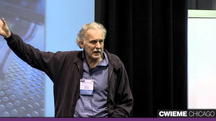
A future possibilities keynote dr walter de heer
Walter Alexander "Walt" de Heer (born November 1949) is a Dutch physicist and nanoscience researcher known for discoveries in the electronic shell structure of metal clusters, magnetism in transition metal clusters, field emission and ballistic conduction in carbon nanotubes, and graphene-based electronics.
Contents
- A future possibilities keynote dr walter de heer
- Academic career
- Research
- Honors and awards
- Letter to Nobel prize committee
- References
Academic career
De Heer earned a doctoral degree in Physics from the University of California, Berkeley in 1986 under the supervision of Walter D. Knight. He worked at the École Polytechnique Fédérale de Lausanne in Switzerland from 1987 to 1997, and is currently a Regents' Professor of Physics at the Georgia Institute of Technology. He directs the Epitaxial Graphene Laboratory in the School of Physics and leads the Epitaxial Graphene Interdisciplinary Research Group at the Georgia Tech Materials Research Science and Engineering Center.
Research
De Heer and his research groups have made significant contributions to several important areas in nanoscopic physics. As a graduate student at UC-Berkeley, he participated in groundbreaking research on alkali metal clusters that demonstrated the electronic shell structure of metal clusters. This is a property of small metal clusters composed of few atoms that develop atom-like electronic properties (these clusters are also referred to as superatoms). In Switzerland, he developed methods of measuring the magnetic properties of cold metal clusters and described how magnetism develops in these clusters as their size increases from atomic to bulk. He is the author of the most highly cited review articles on metallic clusters.
De Heer turned to carbon nanotubes in 1995, showing that they are excellent field emitters, with potential application to flat panel displays. In 1998, he discovered that carbon nanotubes are ballistic conductors at room temperature, meaning that they conduct electrons over relatively large distances without resistance. This is a key selling point of nanotube- and graphene-based electronics.
His nanotube work led to consideration of the properties of "opened" carbon nanotubes and the development of graphene-based electronics, starting in 2001. Anticipating that patterned graphene structures would behave like interconnected carbon nanotubes, he proposed several avenues of graphene preparation, including exfoliation of graphite flakes to oxidized silicon wafers and epitaxial growth on silicon carbide. The latter was deemed most promising for large-scale integrated electronics, and was funded by Intel Corporation in 2003. In 2004, the group was awarded additional funding from the National Science Foundation for the pursuit of graphene science. The first paper, "Two dimensional electron gas properties of ultrathin epitaxial graphite", was presented in March 2004 at a meeting of the American Physical Society and published in December under the title, "Ultrathin epitaxial graphite: Two dimensional electron gas properties and a route towards graphene based electronics". This paper, based primarily on data documented in 2003, describes the first electrical measurements of epitaxial graphene, reports fabrication of the first graphene transistor, and outlines the desirable properties of graphene for use in graphene-based electronics. De Heer and coworkers Claire Berger and Phillip First hold the first patent on graphene-based electronics, provisionally filed in June 2003. The approach championed by de Heer has the advantage of producing graphene directly on a high-quality electronic material (silicon carbide) and does not require isolation or transfer to any other substrate.
Honors and awards
In 2006, de Heer was named as one of the "Scientific American 50", a list of individuals/organizations honored for their contributions to science and society during the preceding year. In 2007, he and his research group were awarded the prestigious W.M. Keck Foundation grant for continuation of work on "nanopatterned epitaxial graphene electronic devices that work at room temperature." De Heer received IBM Faculty Awards in 2007 and 2008, and his work on graphene transistors was named as one of Technology Review's 10 emerging technologies "most likely to change the way we live" in 2008. In September 2009, de Heer was awarded the ACSIN Nanoscience Prize "for his visionary work in developing the field of graphene nanoscience and technology". De Heer has been awarded the 2010 Materials Research Society Medal "for his pioneering contributions to the science and technology of epitaxial graphene". His h-index is currently 71.
Letter to Nobel prize committee
In November 2010, De Heer wrote to the Nobel prize committee criticising certain aspects of the Scientific Background document relating to the award of the Nobel Prize to Andre Geim and Konstantin Novoselov.