
 | ||
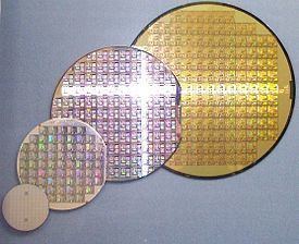
A wafer, also called a slice or substrate, is a thin slice of semiconductor material, such as a crystalline silicon, used in electronics for the fabrication of integrated circuits and in photovoltaics for conventional, wafer-based solar cells. The wafer serves as the substrate for microelectronic devices built in and over the wafer and undergoes many microfabrication process steps such as doping or ion implantation, etching, deposition of various materials, and photolithographic patterning. Finally the individual microcircuits are separated (dicing) and packaged.
Contents
- History
- Formation
- Cleaning texturing and etching
- Standard wafer sizes
- Historical increases of wafer size
- Proposed 450 mm transition
- Analytical die count estimation
- Crystalline orientation
- Crystallographic orientation notches
- Impurity doping
- Compound semiconductors
- References
History
By 1960, silicon wafers were being manufactured in the U.S. by companies such as MEMC/SunEdison. In 1965, American engineers Eric O. Ernst, Donald J. Hurd, and Gerard Seeley, while working under IBM, filed Patent US3423629A for the first high-capacity epitaxial apparatus.
Formation
Wafers are formed of highly pure (99.9999999% purity), nearly defect-free single crystalline material. One process for forming crystalline wafers is known as Czochralski growth invented by the Polish chemist Jan Czochralski. In this process, a cylindrical ingot of high purity mono crystalline semiconductor, such as silicon or germanium, called a boule, is formed by pulling a seed crystal from a 'melt'. Donor impurity atoms, such as boron or phosphorus in the case of silicon, can be added to the molten intrinsic material in precise amounts in order to dope the crystal, thus changing it into n-type or p-type extrinsic semiconductor.
The boule is then sliced with a wafer saw (wire saw) and polished to form wafers. The size of wafers for photovoltaics is 100–200 mm square and the thickness is 200–300 μm. In the future, 160 μm will be the standard. Electronics use wafer sizes from 100–450 mm diameter. (The largest wafers made have a diameter of 450 mm but are not yet in general use.)
Cleaning, texturing and etching
Wafers are cleaned with weak acids to remove unwanted particles, or repair damage caused during the sawing process. When used for solar cells, the wafers are textured to create a rough surface to increase their efficiency. The generated PSG (phosphosilicate glass) is removed from the edge of the wafer in the etching.
Standard wafer sizes
Silicon wafers are available in a variety of diameters from 25.4 mm (1 inch) to 300 mm (11.8 inches). Semiconductor fabrication plants (also known as fabs) are defined by the diameter of wafers that they are tooled to produce. The diameter has gradually increased to improve throughout and reduce cost with the current state-of-the-art fab using 300 mm, with a proposal to adopt 450 mm. Intel, TSMC and Samsung are separately conducting research to the advent of 450 mm "prototype" (research) fabs, though serious hurdles remain.
Wafers grown using materials other than silicon will have different thicknesses than a silicon wafer of the same diameter. Wafer thickness is determined by the mechanical strength of the material used; the wafer must be thick enough to support its own weight without cracking during handling.
Historical increases of wafer size
A unit wafer fabrication step, such as an etch step, can produce more chips proportional to the increase in wafer area, while the cost of the unit fabrication step goes up more slowly than the wafer area. This was the cost basis for increasing wafer size. Conversion to 300 mm wafers from 200 mm wafers began in earnest in 2000, and reduced the price per die about 30-40%. However, this was not without significant problems for the industry.
Proposed 450 mm transition
There is considerable resistance to the 450 mm transition despite the possible productivity improvement, because of concern about insufficient return on investment. Higher cost semiconductor fabrication equipment for larger wafers increases the cost of 450 mm fabs (semiconductor fabrication facilities or factories). Lithographer Chris Mack claimed in 2012 that the overall price per die for 450 mm wafers would be reduced by only 10–20% compared to 300 mm wafers, because over 50% of total wafer processing costs are lithography-related. Converting to larger 450 mm wafers would reduce price per die only for process operations such as etch where cost is related to wafer count, not wafer area. Cost for processes such as lithography is proportional to wafer area, and larger wafers would not reduce the lithography contribution to die cost. Nikon plans to deliver 450-mm lithography equipment in 2015, with volume production in 2017. In November 2013 ASML paused development of 450-mm lithography equipment, citing uncertain timing of chipmaker demand.
The time-line for 450 mm has not been fixed. Mark Durcan, CEO of Micron Technology, said in February 2014 that he expects 450 mm adoption to be delayed indefinitely or discontinued. “I am not convinced that 450mm will ever happen but, to the extent that it does, it’s a long way out in the future. There is not a lot of necessity for Micron, at least over the next five years, to be spending a lot of money on 450mm. There is a lot of investment that needs to go on in the equipment community to make that happen. And the value at the end of the day – so that customers would buy that equipment – I think is dubious.” As of March 2014, Intel Corporation expects 450 mm deployment by 2020 (by the end of this decade). Mark LaPedus of semiengineering.com reported in mid-2014 that chipmakers had delayed adoption of 450 mm “for the foreseeable future.” According to this report some observers expect 2018 to 2020, while “G. Dan Hutcheson, chief executive of VLSI Research, doesn’t see 450mm fabs moving into production until 2020 to 2025.”
The step up to 300 mm required major changes, with fully automated factories using 300 mm wafers versus barely automated factories for the 200 mm wafers. These major investments were undertaken in the economic downturn following the dot-com bubble, resulting in huge resistance to upgrading to 450 mm by the original timeframe. On the ramp up to 450 mm are that the crystal ingots will be 3 times heavier (total weight a metric ton) and take 2–4 times longer to cool, and the process time will be double. All told, the development of 450 mm wafers requires significant engineering, time, and cost to overcome.
Analytical die count estimation
In order to minimize the cost per die, manufacturers wish to maximize the number of dies that can be made from a single wafer; dies always have a square or rectangular shape due to the constraint of wafer dicing. In general, this is a computationally complex problem with no analytical solution, dependent on both the area of the dies as well as their aspect ratio (square or rectangular) and other considerations such as scribeline size and the space occupied by alignment and test structures. Note that gross DPW formulas account only for wafer area that is lost because it cannot be used to make physically complete dies; gross DPW calculations do not account for yield loss due to defects or parametric issues.
Nevertheless, the number of gross die per wafer (DPW) can be estimated starting with the first-order approximation or wafer-to-die area ratio,
where
Refinements of this simple formula typically add an edge correction, to account for partial dies on the edge, which in general will be more significant when the area of the die is large compared to the total area of the wafer. In the other limiting case (infinitesimally small dies or infinitely large wafers), the edge correction is negligible.
The correction factor or correction term generally takes one of the forms cited by De Vries,
Studies comparing these analytical formulas to brute-force computational results show that the formulas can be made more accurate, over practical ranges of die sizes and aspect ratios, by adjusting the coefficients of the corrections to values above or below unity, and by replacing the linear die dimension
Crystalline orientation
Wafers are grown from crystal having a regular crystal structure, with silicon having a diamond cubic structure with a lattice spacing of 5.430710 Å (0.5430710 nm). When cut into wafers, the surface is aligned in one of several relative directions known as crystal orientations. Orientation is defined by the Miller index with (100) or (111) faces being the most common for silicon. Orientation is important since many of a single crystal's structural and electronic properties are highly anisotropic. Ion implantation depths depend on the wafer's crystal orientation, since each direction offers distinct paths for transport. Wafer cleavage typically occurs only in a few well-defined directions. Scoring the wafer along cleavage planes allows it to be easily diced into individual chips ("dies") so that the billions of individual circuit elements on an average wafer can be separated into many individual circuits.
Crystallographic orientation notches
Wafers under 200 mm diameter have flats cut into one or more sides indicating the crystallographic planes of the wafer (usually a {110} face). In earlier-generation wafers a pair of flats at different angles additionally conveyed the doping type (see illustration for conventions). Wafers of 200 mm diameter and above use a single small notch to convey wafer orientation, with no visual indication of doping type.
Impurity doping
Silicon wafers are generally not 100% pure silicon, but are instead formed with an initial impurity doping concentration between 1013 and 1016 atoms per cm3 of boron, phosphorus, arsenic, or antimony which is added to the melt and defines the wafer as either bulk n-type or p-type. However, compared with single-crystal silicon's atomic density of 5×10²² atoms per cm3, this still gives a purity greater than 99.9999%. The wafers can also be initially provided with some interstitial oxygen concentration. Carbon and metallic contamination are kept to a minimum. Transition metals, in particular, must be kept below parts per billion concentrations for electronic applications.
Compound semiconductors
While silicon is the prevalent material for wafers used in the electronics industry, other compound III-V or II-VI materials have also been employed. Gallium arsenide (GaAs), a III-V semiconductor produced via the Czochralski process, is also a common wafer material.