
Produced 2001 Max. CPU clock rate 500 MHz to 1.4 GHz Min. feature size 0.13 to 0.15 | Common manufacturer(s) VIA FSB speeds 100 MHz to 133 MHz | |
 | ||
The VIA C3 is a family of x86 central processing units for personal computers designed by Centaur Technology and sold by VIA Technologies. The different CPU cores are built following the design methodology of Centaur Technology.
Contents
Samuel 2 and Ezra cores
VIA Cyrix III was renamed VIA C3 with the switch to the advanced "Samuel 2" (C5B) core. The addition of an on-die L2 cache improved performance somewhat. As it was not built upon Cyrix technology at all, the new name was just a logical step. To improve power consumption and reduce manufacturing costs, Samuel 2 was produced with 150 nm process technology.
The VIA C3 processor continued an emphasis on minimizing power consumption with the next die shrink to a mixed 130/150 nm process. "Ezra" (C5C) and "Ezra-T" (C5N) were only new revisions of the "Samuel 2" core with some minor modifications to the bus protocol of "Ezra-T" to match compatibility with Intel's Pentium III "Tualatin" cores. VIA enjoyed the lowest power usage in the x86 CPU market for several years. Performance, however, fell behind due to the lack of improvements to the design.
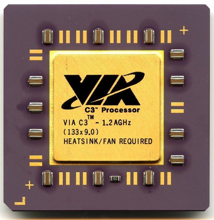
Uniquely, the retail C3 CPU shipped inside a metal package.
Nehemiah cores
The "Nehemiah" (C5XL) was a major core revision. At the time, VIA's marketing efforts did not fully reflect the changes that had taken place. The company addressed numerous design shortcomings of the older cores, including the half-speed FPU. The number of pipeline stages was increased from 12 to 16, to allow for continued increases in clock speed. Additionally, it implemented the cmov instruction, making it a 686-class processor. The Linux kernel refers to this core as the C3-2. It also removes 3DNow! instructions in favour of implementing SSE. However, it was still based upon the aging Socket 370, running the single data rate front side bus at just 133 MHz.
Because the embedded system marketplace prefers low-power, low-cost CPU designs, VIA began targeting this segment more aggressively because the C3 fit those traits rather well. Centaur Technology concentrated on adding features attractive to the embedded marketplace. An example built into the first "Nehemiah" (C5XL) core were the twin hardware random number generators. (These generators are erroneously called “quantum-based” in VIA's marketing literature. Detailed analysis of the generator makes it clear that the source of randomness is thermal, not quantum.)
The "C5P" revision of "Nehemiah" brought with it a few more advancements, including a high-performance AES encryption engine along with a notably small ball grid array chip package the size of a US 1 cent coin.
When this architecture was marketed it was often referred to as the "VIA C5".
Design methodology
While slower than x86 CPUs being sold by AMD and Intel, both in absolute terms and on a clock-for-clock basis, VIA's chips are much smaller, cheaper to manufacture, and lower power. This makes them highly attractive in the embedded marketplace, and increasingly in the mobile sector as well.
This has also enabled VIA to continue to scale the frequencies of their chips with each manufacturing process die shrink, while competitive products from Intel (such as the P4 Prescott) have encountered severe thermal management issues, although the new Intel Core generation of chips are substantially cooler.
To this extent, the performance gap that used to exist between VIA and competing x86 chips is still wide, but starting to narrow. Some of the design trade offs made by the VIA design team are worthy of study, as they run contrary to accepted wisdom.
C3
Contracts
VIA’s embedded platform products have reportedly (2005) been adopted in Nissan’s car series, the Lafesta, Murano, and Presage. These and other high volume industrial applications are starting to generate big profits for VIA as the small form factor and low power advantages close embedded deals.
Legal issues
On the basis of the IDT Centaur acquisition, VIA appears to have come into possession of at least three patents, which cover key aspects of processor technology used by Intel. On the basis of the negotiating leverage these patents offered, in 2003 VIA arrived at an agreement with Intel that allowed for a ten-year patent cross license, enabling VIA to continue to design and manufacture x86 compatible CPUs. VIA was also granted a three-year period of grace in which it could continue to use Intel socket infrastructure.