
 | ||
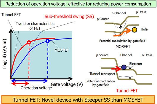
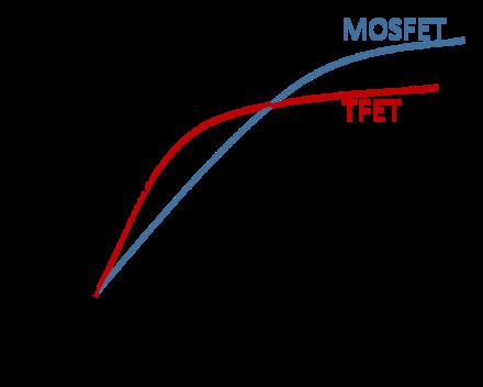
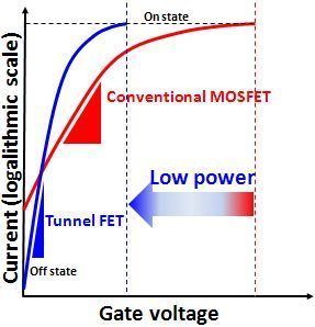
The tunnel field-effect transistor (TFET) is a new type of transistor. Even though its structure is very similar to a metal-oxide-semiconductor field-effect (MOSFET), the fundamental switching mechanism differs, making this device a promising candidate for low energy electronics. TFETs switch by modulating quantum tunneling through a barrier instead of modulating thermionic emission over a barrier as in traditional MOSFETs. Because of this, TFETs are not limited by the thermal Maxwell–Boltzmann tail of carriers, which limits MOSFET drain current subthreshold swing to about 60 mV/decade of current at room temperature (exactly 63 mV/decade at 300 K). Joerg Appenzeller and his colleagues at IBM were the first to demonstrate that current swings below the MOSFET’s 60-mV-per-decade limit were possible. In 2004, they reported they had created a tunnel transistor with a carbon nanotube channel and a subthreshold swing of just 40 mV per decade.
Contents
Theoretical work has indicated that significant power savings can be obtained by using low-voltage TFETs in place of MOSFETs in logic circuits.
In classical MOSFET devices, the 63 mV/decade is a fundamental limit to power scaling. The ratio between on-current and the off-current (especially the subthreshold leakage — one major contributor of power consumption) is given by the ratio between the threshold voltage and the subthreshold slope, e.g.:
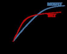
The on-current is proportional to the transistor speed: The higher the on-current, the faster a transistor will be able to charge its fan-out (consecutive capacitive load). For a given transistor speed and a maximum acceptable subthreshold leakage, the subthreshold slope thus defines a certain minimal threshold voltage. Reducing the threshold voltage is an essential part for the idea of constant field scaling. Since 2003, the major technology developers got almost stuck in threshold voltage scaling and thus could also not scale supply voltage (which due to technical reasons has to be at least 3 times the threshold voltage for high performance devices). As a consequence, the processor speed did not develop as fast as before 2003 (see Beyond CMOS). The advent of a mass-producible TFET device with a slope far below 63 mV/decade will enable the industry to continue the scaling trends from the 1990s, where processor frequency doubled each 3 years.
Structure
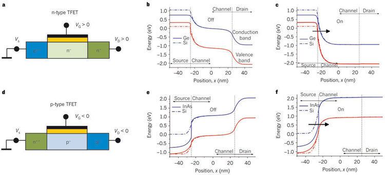
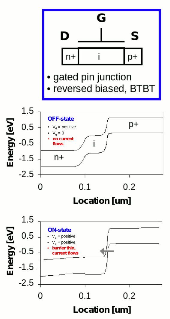
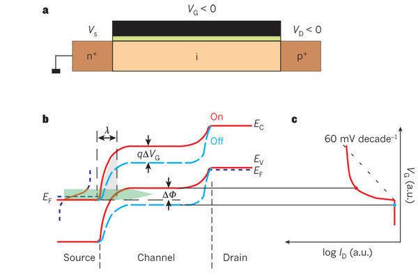
The basic TFET structure is similar to a MOSFET except that the source and drain terminals of a TFET are doped of opposite type (see figure). A common TFET device structure consists of a P-I-N (p-type, intrinsic, n-type) junction, in which the electrostatic potential of the intrinsic region is controlled by a gate terminal.
Device operation
The device is operated by applying gate bias so that electron accumulation occurs in the intrinsic region. At sufficient gate bias, band-to-band tunneling (BTBT) occurs when the conduction band of the intrinsic region aligns with the valence band of the P region. Electrons from the valence band of the p-type region tunnel into the conduction band of the intrinsic region and current can flow across the device. As the gate bias is reduced, the bands becomes misaligned and current can no longer flow.
Prototype devices
A group at IBM were the first to demonstrate that current swings below the MOSFET’s 60-mV-per-decade limit were possible. In 2004, they reported a tunnel transistor with a carbon nanotube channel and a subthreshold swing of just 40 mV per decade.
By 2010, many TFETs have been fabricated in different material systems, but none has yet been able to demonstrate steep subthreshold slope at drive currents required for mainstream applications.
Future work
Double-gate thin-body quantum well-to-quantum well TFET structures have been proposed to overcome some challenges associated with the lateral TFET structure, such as its requirement for ultra sharp doping profiles; however, such devices may be plagued by gate leakage due to large vertical fields in the device structure.
Theory and simulations
Simulations in 2013 showed that TFETs using InAs-GaSb may have a subthreshold swing of 33 mV/decade under ideal conditions.