 | ||
Three dimensional integrated circuit
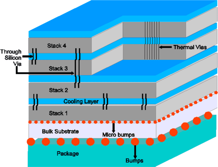
In microelectronics, a three-dimensional integrated circuit (3D IC) is an integrated circuit manufactured by stacking silicon wafers and/or dies and interconnecting them vertically using through-silicon vias (TSVs) so that they behave as a single device to achieve performance improvements at reduced power and smaller footprint than conventional two dimensional processes. 3D IC is just one of a host of 3D integration schemes that exploit the z-direction to achieve electrical performance benefits.
Contents
- Three dimensional integrated circuit
- 3D ICs vs 3D packaging
- 3D SiCs
- Monolithic 3D ICs
- Manufacturing technologies for 3D SiCs
- Benefits
- Challenges
- Design styles
- Notable 3D chips
- References
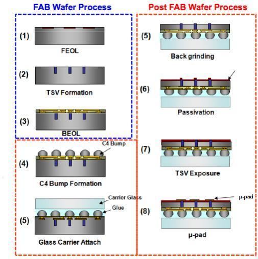
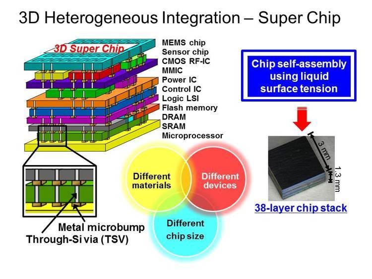
3D integrated circuits can be classified by their level of interconnect hierarchy at the global (package), intermediate (bond pad) and local (transistor) level In general, 3D integration is a broad term that includes such technologies as 3D wafer-level packaging (3DWLP); 2.5D and 3D interposer-based integration; 3D stacked ICs (3D-SICs), monolithic 3D ICs; 3D heterogeneous integration; and 3D systems integration.
International organizations such as the Jisso Technology Roadmap Committee (JIC) and the International Technology Roadmap for Semiconductors (ITRS) have worked to classify the various 3D integration technologies to further the establishment of standards and roadmaps of 3D integration.
3D ICs vs. 3D packaging
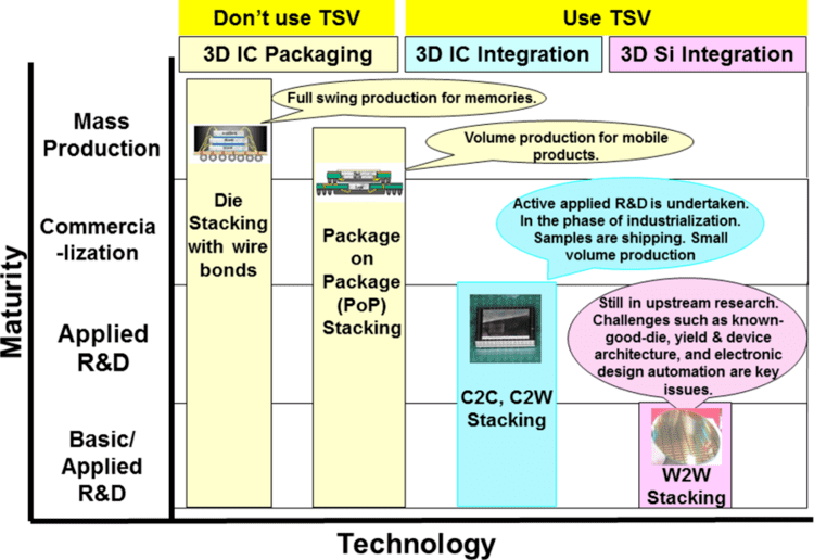
3D Packaging refers to 3D integration schemes that rely on traditional methods of interconnect such as wire bonding and flip chip to achieve vertical stacks. 3D packaging can be disseminated further into 3D system in package (3D SiP) and 3D wafer level package (3D WLP). Stacked memory die interconnected with wire bonds, and package on package (PoP) configurations interconnected with either wire bonds, or flip chips are 3D SiPs that have been in mainstream manufacturing for some time and have a well established infrastructure. PoP is used for vertically integrating disparate technologies such as 3D WLP uses wafer level processes such as redistribution layers (RDL) and wafer bumping processes to form interconnects.
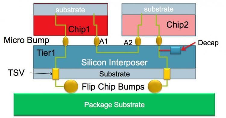
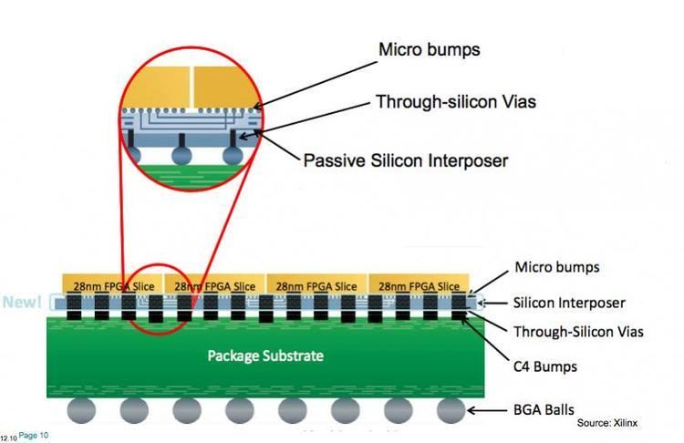
2.5D interposer is also a 3D WLP that interconnects die side-side on a silicon, glass or organic interposer using TSVs and RDL. In all types of 3D Packaging, chips in the package communicate using off-chip signaling, much as if they were mounted in separate packages on a normal circuit board.
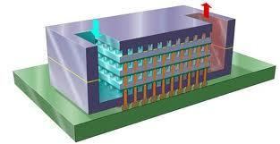
3D ICs can be divided into 3D Stacked ICs (3D SIC), which refers to stacking IC chips using TSV interconnects, and monolithic 3D ICs, which use fab processes to realize 3D interconnects at the local levels of the on-chip wiring hierarchy as set forth by the ITRS, this results in direct vertical interconnects between device layers. The first examples of a monolithic approach are seen in Samsung’s 3D VNAND devices.
3D SiCs
The digital electronics market requires a higher density semiconductor memory chip to cater to recently released CPU components, and the multiple die stacking technique has been suggested as a solution to this problem. JEDEC disclosed the upcoming DRAM technology includes the "3D SiC" die stacking plan at "Server Memory Forum", November 1–2, 2011, Santa Clara, CA. In August 2014, Samsung started producing 64GB DRAM modules for servers based on emerging DDR4 (double-data rate 4) memory using 3D TSV package technology. Newer proposed standards for 3D stacked DRAM include Wide I/O, Wide I/O 2, Hybrid Memory Cube, High Bandwidth Memory.
Monolithic 3D ICs
Monolithic 3D ICs are built in layers on a single semiconductor wafer, which is then diced into 3D ICs. There is only one substrate, hence no need for aligning, thinning, bonding, or through-silicon vias. Process temperature limitations are addressed by partitioning the transistor fabrication to two phases. A high temperature phase which is done before layer transfer follow by a layer transfer use ion-cut, also known as layer transfer, which has been used to produce Silicon on Insulator (SOI) wafers for the past two decades. Multiple thin (10s–100s nanometer scale) layers of virtually defect-free Silicon can be created by utilizing low temperature (<400℃) bond and cleave techniques, and placed on top of active transistor circuitry. Follow by finalizing the transistors using etch and deposition processes. This monolithic 3D IC technology has been researched at Stanford University under a DARPA-sponsored grant.
CEA-Leti is also developing monolithic 3D IC approaches, called sequential 3D IC. In 2014, the French research institute introduced its CoolCube™, a low-temperature process flow that provides a true path to 3DVLSI. At Stanford University, researchers are designing monolithic 3D ICs using carbon nanotube (CNT) structures vs. silicon using a wafer-scale low temperature CNT transfer processes that can be done at 120℃.
In general, monolithic 3D ICs are still a developing technology and are considered by most to be several years away from production.
Manufacturing technologies for 3D SiCs
As of 2014, a number of memory products such as High Bandwidth Memory (HBM) and the Hybrid Memory Cube have been launched that implement 3D IC stacking with TSVs. There are a number of key stacking approaches being implemented and explored. These include die-to-die, die-to-wafer, and wafer-to-wafer.
Benefits
While traditional CMOS scaling processes improves signal propagation speed, scaling from current manufacturing and chip-design technologies is becoming more difficult and costly, in part because of power-density constraints, and in part because interconnects do not become faster while transistors do. 3D ICs address the scaling challenge by stacking 2D dies and connecting them in the 3rd dimension. This promises to speed up communication between layered chips, compared to planar layout. 3D ICs promise many significant benefits, including:
Challenges
Because this technology is new it carries new challenges, including:
Design styles
Depending on partitioning granularity, different design styles can be distinguished. Gate-level integration faces multiple challenges and currently appears less practical than block-level integration.
Notable 3D chips
In 2004 Tezzaron Semiconductor built working 3D devices from six different designs. The chips were built in two layers with "via-first" tungsten TSVs for vertical interconnection. Two wafers were stacked face-to-face and bonded with a copper process. The top wafer was thinned and the two-wafer stack was then diced into chips. The first chip tested was a simple memory register, but the most notable of the set was an 8051 processor/memory stack that exhibited much higher speed and lower power consumption than an analogous 2D assembly.
In 2004, Intel presented a 3D version of the Pentium 4 CPU. The chip was manufactured with two dies using face-to-face stacking, which allowed a dense via structure. Backside TSVs are used for I/O and power supply. For the 3D floorplan, designers manually arranged functional blocks in each die aiming for power reduction and performance improvement. Splitting large and high-power blocks and careful rearrangement allowed to limit thermal hotspots. The 3D design provides 15% performance improvement (due to eliminated pipeline stages) and 15% power saving (due to eliminated repeaters and reduced wiring) compared to the 2D Pentium 4.
The Teraflops Research Chip introduced in 2007 by Intel is an experimental 80-core design with stacked memory. Due to the high demand for memory bandwidth, a traditional I/O approach would consume 10 to 25 W. To improve upon that, Intel designers implemented a TSV-based memory bus. Each core is connected to one memory tile in the SRAM die with a link that provides 12 GB/s bandwidth, resulting in a total bandwidth of 1 TB/s while consuming only 2.2 W.
An academic implementation of a 3D processor was presented in 2008 at the University of Rochester by Professor Eby Friedman and his students. The chip runs at a 1.4 GHz and it was designed for optimized vertical processing between the stacked chips which gives the 3D processor abilities that the traditional one layered chip could not reach. One challenge in manufacturing of the three-dimensional chip was to make all of the layers work in harmony without any obstacles that would interfere with a piece of information traveling from one layer to another.
In ISSCC 2012, two 3D-IC-based multi-core designs using GlobalFoundries' 130 nm process and Tezzaron's FaStack technology were presented and demonstrated. 3D-MAPS, a 64 custom core implementation with two-logic-die stack was demonstrated by researchers from the School of Electrical and Computer Engineering at Georgia Institute of Technology. The second prototype was from the Department of Electrical Engineering and Computer Science at University of Michigan called Centip3De, a near-threshold design based on ARM Cortex-M3 cores.
