
 | ||
Thermal scanning probe lithography (t-SPL) is a form of scanning probe lithography (SPL) whereby material is structured on the nanoscale using scanning probes, primarily through the application of thermal energy.
Contents
Related fields are thermo-mechanical SPL (see also Millipede memory), thermochemical SPL (or thermochemical nanolithography) where the goal is to influence the local chemistry, and thermal Dip Pen Lithography as an additive technique.
History
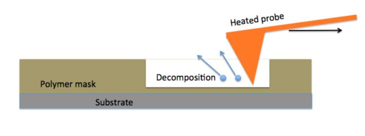
Scientists around Daniel Rugar and John Mamin at the IBM research laboratories in Almaden have been the pioneers in using heated AFM (atomic force microscope) probes for the modification of surfaces. In 1992, they used microsecond laser pulses to heat AFM tips to write indents as small as 150 nm into the polymer PMMA at rates of 100 kHz. In the following years, they developed cantilevers with resonance frequencies above 4 MHz and integrated resistive heaters and piezoresistive sensors for writing and reading of data. This thermo-mechanical data storage concept formed the basis of the Millipede project which was initialized by Peter Vettiger and Gerd Binnig at the IBM Research laboratories Zurich in 1995. It was an example of a memory storage device with a large array of parallel probes, which was however never commercialized due to growing competition from non-volatile memory such as flash memory. The storage medium of the Millipede memory consisted of polymers with shape memory functionality, like e.g. cross-linked polystyrene, in order to allow to write data indents by plastic deformation and erasing of the data again by heating. However, evaporation instead of plastic deformation was necessary for nanolithography applications to be able to create any pattern in the resist. Such local evaporation of resist induced by a heated tip could achieved for several materials like Pentaerythritol tetranitrate, cross-linked polycarbonates, and Diels-Alder polymers. Significant progress in the choice of resist material was made in 2010 at IBM Research in Zurich, leading to high resolution and precise 3D-relief patterning with the use of the self-amplified depolymerization polymer polyphthalaldehyde (PPA) and molecular glasses as resist, where the polymer decomposes into volatile monomers upon heating with the tip without the application of mechanical force and without pile-up or residues of the resist.
Working principle
The thermal cantilevers are fabricated from silicon wafers using bulk- and surface micro-machining processes. Probes have a radius of curvatures below 5 nm, enabling sub-10 nm resolution in the resist. The resistive heating is carried out by integrated micro-heaters in the cantilever legs which are created by different levels of doping. The time constant of the heaters lies between 5 μs to 100 μs. Electromigration limits the longterm sustainable heater temperature to 700–800 °C. The integrated heaters enable in-situ metrology of the written patterns, allowing feedback control, field stitching without the use of alignment markers and using pre-patterned structures as reference for sub-5 nm overlay. Pattern transfer for semiconductor device fabrication including reactive ion etching and metal lift-off has been demonstrated with sub-20 nm resolution.
Comparison to other lithographic techniques
Due to the ablative nature of the patterning process, no development step (as in: selective removal of either the exposed or non-exposed regions of the resist as for e-beam and optical lithography) is needed, neither are optical proximity corrections. Maximum linear writing speeds of up to 20 mm/s have been shown with throughputs in the 104 - 105 μm2 h−1 range which is comparable to single-column, Gaussian-shaped e-beam using HSQ as resist. The resolution of t-SPL is determined by the probe tip shape and not limited by the diffraction limit or by the focal spot size of beam approaches, however, tip-sample interactions during the in-situ metrology process create tip wear, limiting the lifetime of the probes. In order to extend the lifetime of the probe tips, Ultrananocrystalline diamond (UNCD) and Silicon-Carbide (SiC)-coated tips or wear-less floating contact imaging methods have been demonstrated. No electron damage or charging is caused to the patterned surfaces due to the absence of electron or ion beams.