
 | ||
Scanning probe lithography (SPL) describes a set of nanolithographic methods to pattern material on the nanoscale using scanning probes. It is a direct-write, mask-less approach which bypasses the diffraction limit and can reach resolutions below 10 nm. It is considered an alternative lithographic technology often used in academic and research environments. The term scanning probe lithography was coined after the first patterning experiments with scanning probe microscopes (SPM) in the late 1980s.
Contents
- Three dimensional nanoprinting via scanning probe lithography delivered layer by layer deposition
- Classification
- Mechanicalthermo mechanical
- Thermal
- Thermo Chemical
- Dip penthermal dip pen
- Oxidation
- Bias induced
- Current induced
- Comparison to other lithographic techniques
- References
Three dimensional nanoprinting via scanning probe lithography delivered layer by layer deposition
Classification
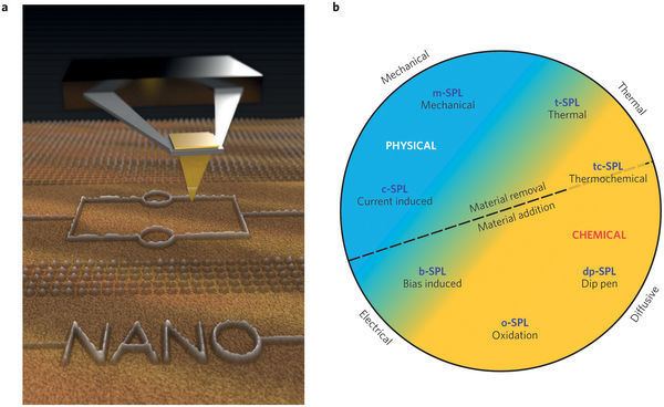
The different approaches towards SPL can be classified by their goal to either add or remove material, by the general nature of the process either chemical or physical, or according to the driving mechanisms of the probe-surface interaction used in the patterning process: mechanical, thermal, diffusive and electrical.
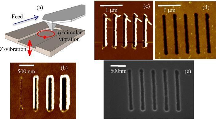
Mechanical/thermo-mechanical
Mechanical scanning probe lithography (m-SPL) is a nanomachining or nano-scratching top-down approach without the application of heat. Thermo-mechanical SPL applies heat together with a mechanical force, e.g. indenting of polymers in the Millipede memory.
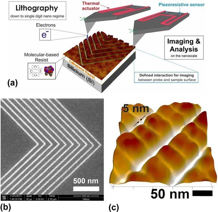
Thermal
Thermal scanning probe lithography (t-SPL) uses a heatable scanning probe in order to efficiently remove material from a surface without the application of significant mechanical forces. The patterning depth can be controlled to create high-resolution 3D structures.
Thermo-Chemical
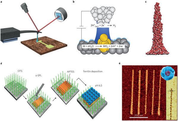
Thermochemical scanning probe lithography (tc-SPL) or thermochemical nanolithography (TCNL) employs the scanning probe tips to induce thermally activated chemical reactions to change the chemical functionality or the phase of surfaces. Such thermally activated reactions have been shown in proteins, organic semiconductors, electroluminescent conjugated polymers, and nanoribbon resistors. Furthermore, deprotection of functional groups (sometimes involving a temperature gradients), reduction of oxides, and the crystallization of piezoelectric/ferroelectric ceramics has been demonstrated.
Dip-pen/thermal dip-pen
Dip-pen scanning probe lithography (dp-SPL) or dip-pen nanolithography (DPN) is a scanning probe lithography technique based on diffusion, where the tip is employed to create patterns on a range of substances by deposition of a variety of liquid inks. Thermal dip-pen scanning probe lithography or thermal dip-pen nanolithography (TDPN) extends the usable inks to solids, which can be deposited in their liquid form when the probes are pre-heated.
Oxidation
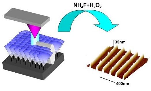
Oxidation scanning probe lithography (o-SPL), also called local oxidation nanolithography (LON), scanning probe oxidation, nano-oxidation, local anodic oxidation, AFM oxidation lithography is based on the spatial confinement of an oxidation reaction.
Bias induced
Bias-induced scanning probe lithography (b-SPL) uses the high electrical fields created at the apex of a probe tip when voltages are applied between tip and sample to facilitate and confining a variety of chemical reactions to decompose gases or liquids in order to locally deposit and grow materials on surfaces.
Current induced
In current induced scanning probe lithography (c-SPL) in addition to the high electrical fields of b-SPL, also a focused electron current which emanates from the SPM tip is used to create nanopatterns, e.g. in polymers and molecular glasses.
Comparison to other lithographic techniques
Being a serial technology, SPL is inherently slower than e.g. photolithography or nanoimprint lithography, while parallelization as required for mass-fabrication is considered a large systems engineering effort (see also Millipede memory). As for resolution, SPL methods bypass the optical diffraction limit due to their use of scanning probes.compared with photolithographic methods. Some probes have integrated in-situ metrology capabilities, allowing for feedback control during the write process. SPL works under ambient atmospheric conditions, without the need for ultra high vacuum (UHV), unlike e-beam or EUV lithography.