
 | ||
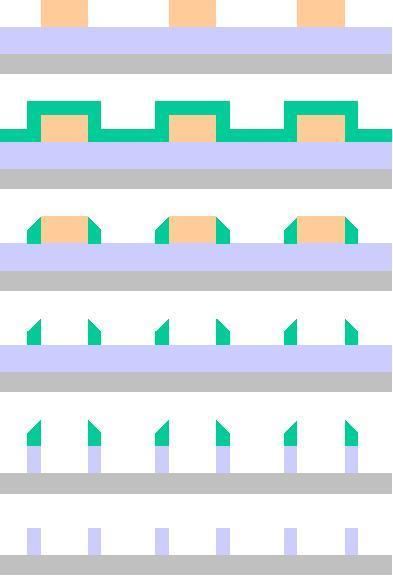
Spacer patterning is a technique employed for patterning features with linewidths smaller than can be achieved by conventional lithography. In the most general sense, the spacer is a layer that is deposited over a pre-patterned feature, often called the mandrel. The spacer is subsequently etched back so that the spacer portion covering the mandrel is etched away while the spacer portion on the sidewall remains. The mandrel may then be removed, leaving two spacers (one for each edge) for each mandrel. The spacers may be further trimmed to narrower widths, especially to act as mandrels for a subsequent 2nd spacer formation. Hence this is a readily practiced form of multiple patterning. Alternatively, one of the two spacers may be removed and the remaining one trimmed to a much smaller final linewidth. Whereas immersion lithography has a resolution of ~40 nm lines and spaces, spacer patterning may be applied to attain 20 nm. This resolution improvement technique is also known as Self-Aligned Double Patterning (SADP). SADP may be re-applied for even higher resolution, and has already been demonstrated for 15 nm NAND flash memory. Spacer patterning has also been adopted for sub-20 nm logic nodes, e.g., 14 nm and 10 nm.
Contents
Spacer Patterning Without Mandrel Removal
The mandrel is not removed after the spacer is etched to leave only the sidewall portion, in the case where the mandrel is the MOSFET gate stack. The silicon nitride sidewall spacer is retained to protect the gate stack and underlying gate oxide during subsequent processing.
Self-Aligned Anti-Spacer Double Patterning
An approach related derived from self-aligned spacer double patterning is so-called "anti-spacer" double patterning. In this approach a first layer coating the mandrel is eventually removed, while a second coated layer over the first layer is planarized and retained. A purely spin-on and wet-processed approached has been demonstrated.
Spacer-Is-Dielectric (SID)
Spacers which define conducting features need to be cut to avoid forming loops. In the alternative spacer-is-dielectric (SID) approach, the spacers define dielectric spaces between conducting features, and so no longer need cuts. The mandrel definition becomes more strategic in the layout, and there is no longer a preference for 1D line-like features. The SID approach has gained popularity due to its flexibility with minimal additional mask exposures. The anti-spacer double patterning approach described above naturally fits the SID approach since an additional layer is deposited after the spacer before its removal.