
 | ||
Scanning tunneling spectroscopy (STS), an extension of scanning tunneling microscopy (STM), is used to provide information about the density of electrons in a sample as a function of their energy.
Contents
In scanning tunneling microscopy, a metal tip is moved over a conducting sample without making mechanical contact. A bias voltage between the sample and tip allows a current to flow between the tip and the sample even though they are not in contact. This can occur because of quantum mechanical tunneling, hence the name of the instrument.
The scanning tunneling microscope is used to obtain "topographs" - topographic maps - of surfaces. The tip is rastered across a surface and (in constant current mode), a constant current is maintained between the tip and the sample by adjusting the height of the tip. A plot of the tip height at all measurement positions on the raster provides the topograph. These topographic images can obtain information that is atomically resolved, and images of metal and semiconductor surfaces can be obtained with atomic precision.
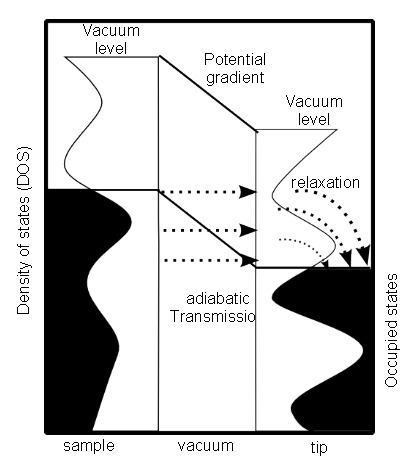
However, the scanning tunneling microscope does not measure the height of surface features. This can be shown when a molecule is adsorbed on a surface. The STM image may appear to have either increased or decreased height at that feature, although the geometry alone is certainly an increased height. A detailed analysis of the way in which an image is formed shows that the transmission of the electric current between the tip and the sample depends on two factors: (1) the geometry of the sample and (2) the arrangement of the electrons in the sample. The arrangement of the electrons in the sample is described quantum mechanically by an "electron density". The electron density is a function of both position and energy, and is formally described as the local density of electron states, abbreviated as local density of states (LDOS), which is a function of energy.
Spectroscopy, in its most general sense, refers to a measurement of the number of something as a function of energy. For scanning tunneling spectroscopy the scanning tunneling microscope is used to measure the number of electrons (the LDOS) as a function of the electron energy. The electron energy is set by the electrical potential difference (voltage) between the sample and the tip. The location is set by the position of the tip.
At its simplest, a "scanning tunneling spectrum" is obtained by placing a scanning tunneling microscope tip above a particular place on the sample. With the height of the tip fixed, the electron tunneling current is then measured as a function of electron energy by varying the voltage between the tip and the sample (the tip to sample voltage sets the electron energy). The change of the current with the energy of the electrons is the simplest spectrum that can be obtained, it is often referred to as an I-V curve. As is shown below, it is the slope of the I-V curve at each voltage (often called the dI/dV-curve) which is more fundamental because dI/dV corresponds to the electron density of states at the local position of the tip, the LDOS.
Introduction
Scanning tunneling spectroscopy (STS) is an experimental technique which uses a scanning tunneling microscope (STM) to probe the local density of electronic states (LDOS) and the band gap of surfaces and materials on surfaces at the atomic scale. Generally, STS involves observation of changes in constant-current topographs with tip-sample bias, local measurement of the tunneling current versus tip-sample bias (I-V) curve, measurement of the tunneling conductance,
Tunneling current
Since STS relies on tunneling phenomena and measurement of the tunneling current or its derivative, understanding the expressions for the tunneling current is very important. Using the modified Bardeen transfer Hamiltonian method, which treats tunneling as a perturbation, the tunneling current (I) is found to be
where
describes the energy lowering due to the interaction between the two states. Here
For low temperatures and a constant tunneling matrix element, the tunneling current reduces to
which is a convolution of the DOS of the tip and the sample. Generally, STS experiments attempt to probe the sample DOS, but equation (3) shows that the tip DOS must be known for the measurement to have meaning. Equation (3) implies that
under the gross assumption that the tip DOS is constant. For these ideal assumptions, the tunneling conductance is directly proportional to the sample DOS.
For higher bias voltages, the predictions of simple planar tunneling models using the Wentzel-Kramers Brillouin (WKB) approximation are useful. In the WKB theory, the tunneling current is predicted to be
where
where
Experimental methods
Acquiring standard STM topographs at many different tip-sample biases and comparing to experimental topographic information is perhaps the most straightforward spectroscopic method. The tip-sample bias can also be changed on a line-by-line basis during a single scan. This method creates two interleaved images at different biases. Since only the states between the Fermi levels of the sample and the tip contribute to
By using modulation techniques, a constant current topograph and the spatially resolved
In order to obtain I-V curves simultaneously with a topograph, a sample-and-hold circuit is used in the feedback loop for the z piezo signal. The sample-and-hold circuit freezes the voltage applied to the z piezo, which freezes the tip-sample distance, at the desired location allowing I-V measurements without the feedback system responding. The tip-sample bias is swept between the specified values, and the tunneling current is recorded. After the spectra acquisition, the tip-sample bias is returned to the scanning value, and the scan resumes. Using this method, the local electronic structure of semiconductors in the band gap can be probed.
There are two ways to record I-V curves in the manner described above. In constant-spacing scanning tunneling spectroscopy (CS-STS), the tip stops scanning at the desired location to obtain an I-V curve. The tip-sample spacing is adjusted to reach the desired initial current, which may be different from the initial current setpoint, at a specified tip-sample bias. A sample-and-hold amplifier freezes the z piezo feedback signal, which holds the tip-sample spacing constant by preventing the feedback system from changing the bias applied to the z piezo. The tip-sample bias is swept through the specified values, and the tunneling current is recorded. Either numerical differentiation of I(V) or lock-in detection as described above for modulation techniques can be used to find
In variable-spacing scanning tunneling spectroscopy (VS-STS), the same steps occur as in CS-STS through turning off the feedback. As the tip-sample bias is swept through the specified values, the tip-sample spacing is decreased continuously as the magnitude of the bias is reduced. Generally, a minimum tip-sample spacing is specified to prevent the tip from crashing into the sample surface at the 0 V tip-sample bias. Lock-in detection and modulation techniques are used to find the conductivity, because the tunneling current is a function also of the varying tip-sample spacing. Numerical differentiation of I(V) with respect to V would include the contributions from the varying tip-sample spacing. Introduced by Mårtensson and Feenstra to allow conductivity measurements over several orders of magnitude, VS-STS is useful for conductivity measurements on systems with large band gaps. Such measurements are necessary to properly define the band edges and examine the gap for states.
Current-imaging-tunneling spectroscopy (CITS) is an STS technique where an I-V curve is recorded at each pixel in the STM topograph. Either variable-spacing or constant-spacing spectroscopy may be used to record the I-V curves. The conductance,
Data interpretation
From the obtained I-V curves, the band gap of the sample at the location of the I-V measurement can be determined. By plotting the magnitude of I on a log scale versus the tip-sample bias, the band gap can clearly be determined. Although determination of the band gap is possible from a linear plot of the I-V curve, the log scale increases the sensitivity. Alternatively, a plot of the conductance,
The structure in the
where
Interpretation of
Since both the tunneling current, equation (5), and the conductance, equation (7), depend on the tip DOS and the tunneling transition probability, T, quantitative information about the sample DOS is very difficult to obtain. Additionally, the voltage dependence of T, which is usually unknown, can vary with position due to local fluctuations in the electronic structure of the surface. For some cases, normalizing
Feenstra et al. argued that the dependencies of
where
Limitations
While STS can provide spectroscopic information with amazing spatial resolution, there are some limitations. The STM and STS lack chemical sensitivity. Since the tip-sample bias range in tunneling experiments is limited to
At finite temperatures, the thermal broadening of the electron energy distribution due to the Fermi-distribution limits spectroscopic resolution. At
where
Despite these limitations, STS and STM provide the possibility for probing the local electronic structure of metals, semiconductors, and thin insulators on a scale unobtainable with other spectroscopic methods. Additionally, topographic and spectroscopic data can be recorded simultaneously.