
Type College Academic staff 50 Number of students 321 | Established 2004 Phone +1 518-437-8686 Founded 2004 | |
 | ||
Academic affiliation State University of New York Officer in charge Alain E. Kaloyeros, Ph.D. Chief academic officer William W. Durgin, Ph.D. Address 257 Fuller Rd, Albany, NY 12203, USA Director Bahgat G. Sammakia (Interim President) Similar SUNY Polytechnic Institute, University at Albany - SUNY, The Sage Colleges, Mohawk Valley Communi, Hudson Valley Communi Profiles | ||
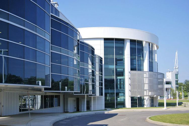
The Colleges of Nanoscale Science and Engineering are the colleges of nanotechnology at the SUNY Polytechnic Institute campus in Albany, New York. Founded in 2004 and formerly a component of the University at Albany, the colleges underwent rapid expansion in the late-2000s and early-2010s before merging with the SUNY Institute of Technology in 2014. As two of five colleges within SUNY Poly, they are the first colleges in the United States devoted to nanotechnology.
Contents
- History
- Academics
- Research centers
- NanoFabs
- Solar Energy Development Center
- Smart Cities Technology Innovation Center
- Marcy Nanocenter
- Computer Chip Commercialization Center
- Central New York Hub for Emerging Nano Industries
- New York Power Electronics Manufacturing Consortium
- Smart System Technology Commercialization Center of Excellence
- Photovoltaic Manufacturing and Technology Development Facility
- Buffalo Medical Innovation and Commercialization Hub
- Buffalo High Tech Manufacturing Innovation Hub at RiverBend
- Buffalo Information Technologies Innovation and Commercialization Hub
- Strategic technology and commercialization centers and programs
- Academic centers and programs
- References
History
The Colleges of Nanoscale Science and Engineering were originally established as the School of Nanosciences and Nanoengineering at the University at Albany in 2001. CNSE was accredited as the College of Nanoscale Science and Engineering of the University at Albany in 2004, and in December of that year, awarded its first Ph.D. degrees in nanoscience. In July 2013, SUNY's Board of Trustees approved a memorandum that led to the separation of CNSE from the University at Albany and included the creation of a new degree-granting structure for the NanoCollege. This was followed by the merger of the SUNY Institute of Technology (SUNYIT) with CNSE in September 2014 to create SUNY Polytechnic Institute. In January 2015, Dr. Alain Kaloyeros was appointed by the SUNY Board of Trustees as the President of SUNY Poly. In September 2016, Kaloyeros was charged with felony bid rigging and subsequently suspended from his job as the Institute's President. In November 2016, Dr. Bahgat Sammakia was named interim President of SUNY Polytechnic Institute by the SUNY Board of Trustees.
Academics
CNSE offers degree programs leading to the Bachelor of Science (B.S.) degree in Nanoscale Engineering and Nanoscale Science, the Master of Science (M.S.) degree in either Nanoscale Science or Nanoscale Engineering, and the Doctor of Philosophy (Ph.D.) degree in either Nanoscale Science or Nanoscale Engineering. CNSE also offers a combined Masters of Science and Masters of Business Administration (M.S.-MBA) degree, the "Nano+MBA," with the ability to earn the M.S. degree in either Nanoscale Science or Nanoscale Engineering, or enroll in the nanotechnology elective track while participating in UAlbany's Evening MBA program. Additionally, CNSE and SUNY Downstate Medical Center offer a joint M.D. and Ph.D. program. The program allows students to earn an M.D. in Medicine and a Ph.D. in Nanoscale Science or Engineering. In 2010, CNSE became the first college in the U.S. to launch a comprehensive baccalaureate program in Nanoscale Engineering and Nanoscale Science. Through the Spring 2013 semester, CNSE has 191 alumni.
Research centers
SUNY Poly CNSE is located near Western Avenue and Fuller Road, west of the University at Albany. The college has a number of wafer fabrication cleanrooms with different classifications for cleanroom suitability.
NanoFabs
NanoFab 200, an earlier part of the campus, was completed in 1997. This 70,000-square-foot (6,500 m2), $16.5 million facility includes 4,000 square feet (370 m2) of cleanroom space, plus CNSE metrology labs and office space for programs such as SUNY’s Atmospheric Sciences Research Center.
NanoFab South, completed March 2004, is a 150,000-square-foot (14,000 m2), $50 million facility including 32,000 square feet (3,000 m2) of 300 mm wafer, class 1-capable cleanroom space.
Completed December 2005, NanoFab North is a 230,000-square-foot (21,000 m2), $175 million facility including 35,000 square feet (3,300 m2) of cleanroom space with Class 1-capable 300mm wafer production.
In March 2009, another $150 million expansion project included NanoFab East, a 250,000-square-foot (23,000 m2) office, laboratory, and classroom building, in addition to NanoFab Central, a separate 100,000-square-foot (9,300 m2) building that houses 15,000 square feet (1,400 m2) of 300mm wafer, class 1-capable cleampus consists of NanoFab Xtension (NFX) which hosts the Global 450mm Consortium as well as an additional 50,000 square feet (4,600 m2) of Class 1 capable cleanroom space, and the Zero Energy Nanotechnology (ZEN) building, a living laboratory for green energy technologies. The expansion will enable the addition of more than 1,000 scientists, researchers, and engineers from CNSE and global corporations.
Solar Energy Development Center
Located in Halfmoon, New York, the Solar Energy Development Center is an 18,000-square-foot (1,700 m2) facility features a state-of-the-art, 100 kilowatt prototyping and demonstration line for next-generation copper indium gallium selenide (CIGS) thin film solar cells, offering critical opportunities to demonstrate emerging concepts in CIGS manufacturing, such as evaluations of innovative materials and novel processes. CNSE's SEDC also supports the U.S. Photovoltaic Manufacturing Consortium, a more than $300 million public-private collaboration headquartered at CNSE.
Smart Cities Technology Innovation Center
Located in Kiernan Plaza the facility specializes in smart devices, sensors and computer chips, integrated systems, and operating software that collect and analyze data for monitoring highway conditions and improving traffic flow; protecting infrastructure such as bridges, data centers, and utility installations; safeguard facilities, including wastewater treatment plants; and provide e-safety and security in educational settings.
Marcy Nanocenter
The development of the Marcy Nanocenter site in Utica is led by CNSE in partnership with quasi-public Mohawk Valley EDGE to accelerate the attraction of 450mm computer chip manufacturing to the Mohawk Valley. The development plan of the Marcy Nanocenter site includes up to 8.25 million square feet of teaching facilities, with up to three 450mm computer chip fabs, each with a cleanroom of approximately 450,000 square feet, a total public and private investment of $10B to $15B for each phase of development, and the creation of approximately 5,000 direct jobs and approximately 15,000 indirect jobs.
Computer Chip Commercialization Center
The Computer Chip Commercialization Center, or Quad C, is located on the SUNY Poly Utica campus, and has an anchor tenant of General Electric.
Central New York Hub for Emerging Nano Industries
Located in Syracuse, the Central New York Hub for Emerging Nano Industries specializes in providing visual production research and education to support New York’s film and television industry, with a focus on the use of nanotechnology to drive innovations in computer-generated imagery and animation, as well as motion capture technology utilized by today’s production facilities. This initiative includes a minimum private investment of $150M over seven years. SUNY Poly will provide $15M to build the facility at the Collamer Crossings Business Park in Dewitt, and Onondaga County has invested $1.4M to ensure shovel-ready status for the two 52,000 square foot buildings, offering research and development, manufacturing, and office space for a diverse cross-section of businesses, including The Film House, a California-based film and television company, which will be the facility’s first tenant. As announced by Andrew Cuomo in March 2014, the project will create at least 350 new jobs and 150 construction jobs.
New York Power Electronics Manufacturing Consortium
located in Rochester, NY, will invest over $500 million and create thousands of high-skilled, high-paying jobs in Upstate New York over the next five years – including at least 500 in Rochester. This public-private partnership will help develop the next generation of materials used on semiconductors at State-owned R&D facilities. Managed by CNSE, the development of this next generation of semiconductors will enable power devices to get smaller, faster and more efficient.
Smart System Technology & Commercialization Center of Excellence
located outside of Rochester in Canandaigua, New York, was created in 2010 through a merger of two of New York State's Centers of Excellence: Infotonics Technology Center (ITC) in Canandaigua and the Center of Excellence in Nanoelectronics and Nanotechnology at CNSE, and offers state-of-the-art capabilities for MEMS fabrication and packaging at its 120,000-square-foot (11,000 m2) facility that includes 26,000 square feet (2,400 m2) of certified cleanroom space with 150mm and 200mm MEMS foundry services, complemented by a dedicated 8,000-square-foot (740 m2) MEMS and optoelectronic packaging facility. The STC positions New York State as a global leader in smart system and smart device innovation and manufacturing and also positions CNSE as a vertically integrated "one-stop-shop" for smart systems' device development and process manufacturing, coupling CNSE's preeminence in nanoelectronics R&D with ITC's expertise in integrating computer chips with hundreds of mechanical devices.
Photovoltaic Manufacturing and Technology Development Facility
to be located inside a 57,000-square-foot (5,300 m2) former Kodak building in the Canal Ponds Business Park in Rochester, New York, is part of a taxpayer-funded $100 million initiative creating the solar industry’s first full-service collaborative space dedicated to advancing crystalline silicon, technologies. Further leveraging the publicly led industry-university partnership model utilized at CNSE, the CNSE MDF will include a state-of-the-art, 20,000-square-foot (1,900 m2) cleanroom instruction center and will provide a range of services and equipment, including complete manufacturing lines, access to individual tools, secure fab space for users’ proprietary tools, and pilot production services in an intellectual property (IP) secure environment. Over $19 million in cutting-edge tools and equipment that are critical to the U.S. Department of Energy’s (DOE) SunShot initiative and which were formerly utilized by SVTC, a Silicon Valley-based solar energy company, will be relocated to the CNSE MDF to constitute the foundation of the manufacturing development line. The CNSE MDF will also enable education and training to support the expansion of the highly skilled workforce required by the U.S. PV manufacturing industry and, in addition, will complement and expand the capabilities and expertise of the national U.S. Photovoltaic Manufacturing Consortium (PVMC), headquartered at CNSE as part of the DOE’s SunShot Initiative.
Buffalo Medical Innovation and Commercialization Hub
Located at the Buffalo Niagara Medical Campus in Buffalo, the Buffalo Medical Innovation and Commercialization Hub is a facility for research, development, and testing for drug screening, pharmaceutical development, technology optimization, business attraction, workforce training, and bioinformatics. This $250 million initiative, with $200 million to be generated by private industry investment and $50 million being invested by New York State, $35 million of which will go toward new equipment and $15 million of which will go toward improving existing lab space, will support over 250 jobs on site.
Buffalo High-Tech Manufacturing Innovation Hub at RiverBend
In 2014, SolarCity invested $5 billion to establish a one million-square-foot factory which will produce solar panels, at the Buffalo High-Tech Manufacturing Innovation Hub at RiverBend, the former site of a Republic Steel factory. It will be the largest facility of its kind in the Western Hemisphere, with more than 1 gigawatt of annual solar capacity when it reaches full production. More than 3,000 jobs will be created in Western New York and a total of nearly 5,000 jobs throughout New York.
Buffalo Information Technologies Innovation and Commercialization Hub
The Buffalo Information Technologies Innovation and Commercialization Hub was created through a $55 million investment by New York. IBM will be the first anchor tenant in the hub and will train information technology professionals and develop software needed in the areas of molecular research, genomics, energy efficiency and defense. Through the hub, IBM will bring 500 new information technology jobs to Buffalo.
Strategic technology and commercialization centers and programs
CNSE is the home of numerous pioneering nanotechnology programs funded by a variety of public and private sources. CNSE is able to accelerate the commercialization of technologies by providing technology deployment, market development, economic outreach and business assistance under a variety of centers and programs.