
 | ||
Resistive random-access memory (RRAM or ReRAM) is a type of non-volatile (NV) random-access (RAM) computer memory that works by changing the resistance across a dielectric solid-state material often referred to as a memristor. This technology bears some similarities to conductive-bridging RAM (CBRAM), and phase-change memory (PCM).
Contents
- History
- Forming
- Operation styles
- Material systems for resistive memory cells
- Demonstrations
- HfO2 based RRAM
- Panasonic
- HP Memristor
- Adesto Technologies
- Crossbar
- 3D XPoint
- Future applications
- References
CBRAM involves one electrode providing ions that dissolve readily in an electrolyte material, while PCM involves generating sufficient Joule heating to effect amorphous-to-crystalline or crystalline-to-amorphous phase changes. On the other hand, RRAM involves generating defects in a thin oxide layer, known as oxygen vacancies (oxide bond locations where the oxygen has been removed), which can subsequently charge and drift under an electric field. The motion of oxygen ions and vacancies in the oxide would be analogous to the motion of electrons and holes in a semiconductor.
RRAM is currently under development by a number of companies, some of which have filed patent applications claiming various implementations of this technology. RRAM has entered commercialization on an initially limited KB-capacity scale.
Although anticipated as a replacement technology for flash memory, the cost benefit and performance benefit of RRAM have not been enough for companies to proceed with the replacement. A broad range of materials apparently can potentially be used for RRAM. However, the recent discovery that the popular high-κ gate dielectric HfO2 can be used as a low-voltage RRAM has greatly encouraged others to investigate other possibilities. Even more recently SiOx has been identified to offer significant benefits. Weebit-Nano Ltd is one company that is pursuing SiOx and has already demonstrated functional devices.
History
In February 2012 Rambus bought an RRAM company called Unity Semiconductor for $35 million. Panasonic launched an RRAM evaluation kit in May 2012, based on a tantalum oxide 1T1R (1 transistor – 1 resistor) memory cell architecture.
In 2013, Crossbar introduced an RRAM prototype as a chip about the size of a postage stamp that could store 1 TB of data. In August 2013, the company claimed that large-scale production of their RRAM chips was scheduled for 2015. The memory structure (Ag/a-Si/Si) closely resembles a silver-based CBRAM.
Different forms of RRAM have been disclosed, based on different dielectric materials, spanning from perovskites to transition metal oxides to chalcogenides. Silicon dioxide was shown to exhibit resistive switching as early as 1967, and has recently been revisited.
Leon Chua argued that all two-terminal non-volatile memory devices including RRAM should be considered memristors. Stan Williams of HP Labs also argued that RRAM was a memristor. However, others challenged this terminology and the applicability of memristor theory to any physically realizable device is open to question. Whether redox-based resistively switching elements (RRAM) are covered by the current memristor theory is disputed.
In 2014 researchers announced a device that used a porous silicon oxide dielectric with no edge structure. In 2010 conductive filament pathways were discovered, leading to the later advance. It can be manufactured at room temperature and has a sub-2V forming voltage, higher on-off ratio, lower power consumption, nine-bit capacity per cell, higher switching speeds and improved endurance.
Forming
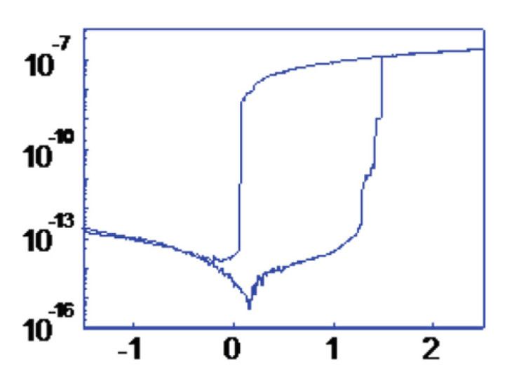
The basic idea is that a dielectric, which is normally insulating, can be made to conduct through a filament or conduction path formed after application of a sufficiently high voltage. The conduction path can arise from different mechanisms, including vacancy or metal defect migration. Once the filament is formed, it may be reset (broken, resulting in high resistance) or set (re-formed, resulting in lower resistance) by another voltage. Many current paths, rather than a single filament, are possibly involved. The presence of these current paths in the dielectric can be in situ demonstrated via conductive atomic force microscopy.
The low-resistance path can be either localized (filamentary) or homogeneous. Both effects can occur either throughout the entire distance between the electrodes or only in proximity to one of the electrodes. Filamentary and homogenous switching effects can be distinguished by measuring the area dependence of the low-resistance state.
Under certain conditions, the forming operation may be bypassed. It is expected that under these conditions, the initial current is already quite high compared to insulating oxide layers.
CBRAM cells generally would not require forming if Cu ions are already present in the electrolyte, having already been driven-in by a designed photo-diffusion or annealing process; such cells may also readily return to their initial state. In the absence of such Cu initially being in the electrolyte, the voltage would still be applied directly to the electrolyte, and forming would be a strong possibility.
Operation styles
For random-access type memories, a 1T1R (one transistor, one resistor) architecture is preferred because the transistor isolates current to cells that are selected from cells that are not. On the other hand, a cross-point architecture is more compact and may enable vertically stacking memory layers, ideally suited for mass-storage devices. However, in the absence of any transistors, isolation must be provided by a "selector" device, such as a diode, in series with the memory element or by the memory element itself. Such isolation capabilities are inferior to the use of transistors if the on/off ratio for the selector is not sufficient, limiting the ability to operate very large arrays in this architecture. Thin film based threshold switch can work as a selector for bipolar and unipolar RRAM. Threshold switch-based selector was demonstrated for 64 Mb array. However, One shouldn't forget that the cross-point architecture requires BEOL compatible two terminal selectors like punch-through diode for bipolar RRAM or PIN diode for unipolar RRAM.
Polarity can be either binary or unary. Bipolar effects cause polarity to reverse when switching from low to high resistance (reset operation) compared to switching high to low (set operation). Unipolar switching leaves polarity unaffected, but uses different voltages.
Material systems for resistive memory cells
Multiple inorganic and organic material systems display thermal or ionic resistive switching effects. These can be grouped into the following categories:
2Sb
2Te
5 or AgInSbTe
2
3 or PCMO
x or Cu
2S
Demonstrations
Papers at the IEDM Conference in 2007 suggested for the first time that RRAM exhibits lower programming currents than PRAM or MRAM without sacrificing programming performance, retention or endurance. Some commonly cited ReRAM systems are described further below.
HfO2-based RRAM
At IEDM 2008, the highest-performance RRAM technology to date was demonstrated by ITRI using HfO2 with a Ti buffer layer, showing switching times less than 10 ns and currents less than 30μA. At IEDM 2010, ITRI again broke the speed record, showing <0.3 ns switching time, while also showing process and operation improvements to allow yield up to 100% and endurance up to 10 billion cycles. IMEC presented updates of their RRAM program at the 2012 Symposia on VLSI Technology and Circuits, including a solution with a 500 nA operating current.
ITRI had focused on the Ti/HfO2 system since its first publication in 2008. ITRI's patent 8362454 has since been sold to TSMC; the number of prior licensees is unknown. On the other hand, IMEC focused mainly on Hf/HfO2. Winbond had done more recent work toward advancing and commercializing the HfO2-based RRAM.
Panasonic
Panasonic revealed its TaOx-based ReRAM at IEDM 2008. A key requirement was the need for a high work function metal such as Pt or Ir to interface with the TaOx layer. The change of O content results in resistance change as well as Schottky barrier change. More recently, a Ta2O5/TaOx layer was implemented, which still requires the high work function metal to interface with Ta2O5. This system has been associated with high endurance demonstration (trillion cycles), but products are specified at 100K cycles. Filament diameters as large as ~100 nm have been observed. Panasonic released a 4Mb part with Fujitsu, and is developing 40nm embedded memory with UMC.
HP Memristor
On 30 April 2008, HP announced that they had discovered the memristor, originally envisioned as a missing 4th fundamental circuit element by Chua in 1971. On 8 July they announced they would begin prototyping RRAM using their memristors. HP first demonstrated its memristor using TiOx, but later migrated to TaOx, possibly due to improved stability. The TaOx-based device has some material similarity to Panasonic's ReRAM, but the operation characteristics are different. The Hf/HfOx system was similarly studied.
Adesto Technologies
Adesto Technologies' ReRAM is based on filaments generated from the electrode metal rather than oxygen vacancies. The original material system was Ag/GeS2 but eventually migrated to ZrTe/Al2O3. The tellurium filament achieved better stability as compared to silver. Adesto has targeted the ultralow power memory for Internet-of-Things (IoT) applications. Adesto has released products manufactured at Altis foundry and entered into a 45nm foundry agreement with TowerJazz/Panasonic.
Crossbar
Crossbar implements an Ag filament in amorphous Si along with a threshold switching system to achieve a diode+ReRAM. Their system includes the use of a transistor in 1T1R or 1TNR architecture. Crossbar has recently started producing samples at SMIC on the 40nm process. The Ag filament diameter has been visualized on the scale of tens of nanometers.
3D XPoint
3D XPoint is not typically associated with ReRAM, but is a resistance change memory more similar to phase change memory. Intel and Micron are the main distributors, first targeting SSD products, and eventually DIMMs. Endurance is 21x that of NAND Flash, with latency of <10 us.
Future applications
Compared to PRAM, RRAM operates at a faster timescale (switching time can be less than 10 ns), while compared to MRAM, it has a simpler, smaller cell structure (less than 8F² MIM stack). A vertical 1D1R (one diode, one resistive switching device) integration can be used for crossbar memory structure to reduce the unit cell size to 4F² (F is the feature dimension). Compared to flash memory and racetrack memory, a lower voltage is sufficient, and hence it can be used in low-power applications. Also, due to its relatively small access latency and high density, RRAM is considered a promising candidate for designing caches.
ITRI has shown that RRAM is scalable below 30 nm. The motion of oxygen atoms is a key phenomenon for oxide-based RRAM; one study indicated that oxygen motion may take place in regions as small as 2 nm. It is believed that if a filament is responsible, it would not exhibit direct scaling with cell size. Instead, the current compliance limit (set by an outside resistor, for example) could define the current-carrying capacity of the filament.
A significant hurdle to realizing the potential of RRAM is the sneak path problem that occurs in larger passive arrays. In 2010, complementary resistive switching (CRS) was introduced as a possible solution to sneak-path current interference. In the CRS approach, the information storing states are pairs of high- and low-resistance states (HRS/LRS and LRS/HRS) so that the overall resistance is always high, allowing larger passive crossbar arrays.
A drawback to the initial CRS solution is the requirement for switching endurance caused by conventional destructive readout based on current measurements. A new approach for a nondestructive readout based on capacity measurement potentially lowers the requirements for both material endurance and power consumption. Bi-layer structure is used to produce the nonlinearity in LRS to avoid the sneak path problem. A single-layer device exhibiting a strong nonlinear conduction in LRS was reported. Another bi-layer structure was introduced for bipolar RRAM to improve the HRS and stability.
Another solution to the sneak current issue is to perform read and reset operations in parallel across an entire row of cells, while using set on selected cells. In this case, for a 3D-RRAM 1TNR array, with a column of N RRAM cells situated above a select transistor, only the intrinsic nonlinearity of the HRS is required to be sufficiently large, since the number of vertical levels N is limited (e.g., N = 8–32), and this has been shown possible for a low-current RRAM system.
Modeling of 2D and 3D caches designed with RRAM and other non-volatile random access memories such as MRAM and PCM can be done using DESTINY tool.