
 | ||
Conductive atomic force microscopy (C-AFM) or current sensing atomic force microscopy (CS-AFM) is a mode in atomic force microscopy (AFM) that simultaneously measures the topography of a material and the electric current flow at the contact point of the tip with the surface of the sample. The topography is measured by detecting the deflection of the cantilever using an optical system (laser + photodiode), while the current is detected using a current-to-voltage preamplifier. The fact that the CAFM uses two different detection systems (optical for the topography and preamplifier for the current) is a strong advantage compared to scanning tunneling microscopy (STM). Basically, in STM the topography picture is constructed based on the current flowing between the tip and the sample (the distance can be calculated depending on the current). Therefore, when a portion of a sample is scanned with an STM, it is not possible to discern if the current fluctutations are related to a change in the topography (due to surface roughness) or to a change in the sample conductivity (due to intrinsic inhomogeneities).
Contents
The CAFM is usually operated in contact mode; the tip can be kept at one location while the voltage and current signals are applied/read, or it can be moved to scan a specific region of the sample under a constant voltage (and the current is collected). Recently, some manufacturers provide the option of measuring the current in semi-contact mode. The CAFM was firstly developed by John O'Shea and co-workers at the University of Cambridge in 1993, and it has been referred in the literature with several names, including C-AFM, local-conductivity AFM (LC-AFM), conductive probe AFM (CP-AFM), conductive scanning probe microscope (C-SPM) or conductive scanning force microscope (C-SFM), although CAFM is the most widespread.
Working principle
In order to transform an AFM into a CAFM, three elements are required: i) the probe tip must be conductive, ii) a voltage source is needed to apply a potential difference between the tip and the sample holder, and iii) a preamplifier is used to convert the (analogical) current signal into (digital) voltages that can be read by the computer. In CAFM experiments, the sample is usually fixed on the sample holder using a conductive tape or paste, being silver paints the most widespread. A Faraday cage is also convenient to isolate the sample from any external electrical interference. Using this setup, when a potential difference is imposed between tip and sample an electrical field is generated, which results in a net current flowing from tip-to-sample or vice versa. The currents collected by the CAFM obey the relationship:
where I is the total current flowing through the tip/sample nanojunction, J is the current density and Aeff is the effective emission area though which electrons can flow (from now on we will refer to it just as effective area). The most common mistake in CAFM research is to assume that the effective emission area (Aeff) equals the physical contact area (Ac). Strictly, this assumption is erroneous because in many different tip/sample systems the electrical field applied may propagate laterally. For example, when the CAFM tip is placed on a metal the lateral conductivity of the sample is very high, making (in principle) the whole sample surface area electrically connected (Aeff equals the area covered by the metallic film/electrode). Aeff has been defined as:"the sum of all those infinitesimal spatial locations on the surface of the sample that are electrically connected to the CAFM tip (the potential difference is negligible). As such, Aeff is a virtual entity that summarizes all electrically relevant effects within the tip/sample contact system into a single value, over which the current density is assumed to be constant." Therefore, when the CAFM tip is placed in contact with a metal (a metallic sample or just a metallic pad on an insulator), the lateral conductivity of the metal is very high, and the CAFM tip can be understood as a current collector (nanosized probestation); on the contrary, if the CAFM tip is placed directly on an insulator, it acts as a nanosized electrode and provides a very high lateral resolution. The value of Aeff when a Pt-Ir coated tip (with a typical radius of 20 nm) is placed on a SiO2 insulating film has been calculated to be typically 50 nm2. The value of Aeff can fluctuate depending on the environmental conditions, and it can range from 1 nm2 in ultra high vacuum (UHV) to 300 nm2 in very humid environments.
Applications
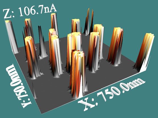
The CAFM was initially used in the field of nanoelectronics to monitor the electrical properties of thin dielectrics with very high lateral resolution. The first CAFM development in 1993 had the goal of studying the local tunneling currents through 12 nm thick SiO2 films. In 1995 and 1996, O'Shea and Ruskell further improved the lateral resolution of the CAFM technique, achieving values of 10 nm and 8 nm, respectively. This enhanced resolution allowed to observe the first topographic-current correlations, and the inhomogeneity observed in the current maps was associated to the presence of local native defects in the oxide. Following works by Olbrich and Ebersberger reported that, in SiO2 films thinner than 5 nm, the tunneling current increases exponentially with thickness reductions. Consequently, thickness fluctuations of tenths of nanometer in the SiO2 film could create electrically weak spots that reduce the reliability of the whole dielectric film, as the dielectric breakdown (BD) is a stochastic process. The capability of the CAFM for determining the thickness of thin oxides was further demonstrated by Frammelsberger and co-workers who statistically analyzed more than 7200 I-V curves, and reported SiO2 thicknesses with a sensitivity of ±0.3 nm. Other local phenomena like charge trapping, trap assisted tunneling and stress induced leakage current (SILC) can be also easily monitored with CAFM. In general, the CAFM can monitor the effect of any process that introduces local changes in the structure of the dielectric, including thermal annealing, dopping and irradiation, among others.
Apart from monitoring the electrical properties of a dielectric, the CAFM can be also used to alter its properties by applying an electrical field locally. In particular, the CAFM is especially useful to determine which locations of the samples lead to premature BD, which can provide essential information about the reliability of the samples. The CAFM also helped to confirm the percolation theory of the BD by experimentally proving that this is a very local phenomenon that occurs in small areas typically below 100 nm2. Lateral propagations of the BD event can also be detected by CAFM. The severity of the BD event can also be studied from the dielectric breakdown induced epitaxy, which can be observed from subsequent topographic images collected with the CAFM after the voltage ramp. Similarly, the analysis of the BD recovery (resistive switching, RS) can also be monitored by CAFM. All the capabilities of the CAFM for studying resistive switching in dielectrics have been summarized in the review article of reference. Unlike a normal AFM, the CAFM can be also used to perform local photolithography via bias-assisted local anodic oxidation (LAO). Nowadays the CAFM technique has expanded to many other fields of science, including physics, materials science, chemistry and engineering (among many others), and it has been used to study different materials and/or structures, including nanoparticles, molecules, nanowires, carbon nanotubes, two dimensional (2D) materials, coatings, photoelectricity and piezoelectricity (among others). As of June 14th of 2016, the CAFM had been used in 1325 journal research articles, and it has become a popular tool in nanosciences.
CAFM probes
The main problem of the CAFM is that the probes are more expensive and wear faster than those used in topographic AFM maps, mainly due to the high current densities flowing through the tip/sample nanojunction, but also due to lateral frictions. The premature degradation of a CAFM tip not only increases the cost of the research, but also reduces the reliability of the data collected. For this reason, when using CAFM, tip conductivity characterization (using a reference sample) before and after the experiments is highly recommended; only if the CAFM tip holds the same conductivity before and after the expeiments, the data collected are trustable. The first types of conductive nanoprobes used in CAFM experiments, which are still widely used nowadays, consist on standard silicon nanoprobes (as those used in topographic AFM measurements) varnished with thin metallic films, including Pt, Au, Ru, Ti and Cr, among others. The thickness of the varnish should be thick enough to withstand the large current densities and frictions, and at the same time thin enough to not increase significantly the radius of the tip apex, maintaining its sharpness and ensuring a high lateral resolution of the CAFM technique. As mentioned, the lifetime of the metal-varnished tips for CAFM experiments is much shorter than in any other AFM mode, mainly due to metallic varnish melting and loss of tip mass during the scans. To solve this problem, CAFM silicon tips varnished with hard materials like phosphorus-doped diamond have appeared. The main problems of diamond-coapted CAFM tips are: i) they are much more expensive, and ii) they are very stiff and can damage (scratch) the surface of the samples under tests. Another option is to use sharpened metallic wires as tip, but also the use of hone techniques increases their price (compared to metal-coated Si tips). Furthermore, these tips can also degrade (lose their conductivity) by particles adhesion. A cheap and effective methodology to protect CAFM tips from degradation is to coat them with graphene, which can withstanding well the high current densities and frictions. Moreover, graphene is inert and slows down particles adhesion to the tip apex.
The preamplifier
The analogical current signals flowing through the tip/sample nanojunction are sent to the preamplifier, which transforms them into digital voltages that can be read by the data acquisition (DAQ) card of the computer. Many manufacturers integrate the preamplifier in the so called "CAFM application module", which is a removable component that can be fixed to the AFM (usually very near to the tip to minimize the electrical noise) to perform conductivity measurements. Similarly, many other modules allow AFMs to perform other operations, like scanning capacitance microscopy (SCM) or scanning spreading resistance microscopy (SSRM). In most CAFM experiments the currents measured typically can range between a few picoamperes and hundreds of microamperes, while the voltages readable by the DAQ card usually range between -3 V to +3V. Therefore, the preamplifier needs to provide a very low noise and a high transimpedance (gain). Figure 2 shows the simplified schematic of a typical low noise preamplifier for CAFM measurements, in which some elements can be distinguished: i) an operational amplifier with high input impedance; ii) a feedback resistor (Rf) and its parasite capacitor (Cs) and Johnson noise (et) associated effects; iii) a noise voltage source associated to the operational amplifier (en); and iv) a capacitance associated to the input interconnections (Ci). A correct selection of the electrical components is essential to achieve good and reliable CAFM data acquisition. For example, the value of Rf is not trivial: a very high value of Rf improves the noise-signal ratio, while reduces the bandwidth of the preamplifier. Therefore, the value of Rf should be chosen to provide enough bandwidth and a noise level below the current values that we want to measure. The parameter en can be easily reduced by using a commercial low noise operational amplifier. The capacitance associated to the connections (Ci) can be easily minimized by placing the preamplifier as near as possible to the conductive tip. The company FEMTO, one of the world leading manufacturers of preamplifiers compatible with CAFMs, can provide devices with electrical noise as low as 3 fA and a gain up to 1013 V/A. Nevertheless, the main limitation of CAFM preamplifiers is their narrow current dynamic range, which usually allows collecting electrical signals only within three or four orders of magnitude (or even less). To solve this problem preamplifiers with an adjustable gain can be used to focus on specific ranges. A more sophisticated solution for this problem is to combine the CAFM with a sourcemeter, semiconductor parameter analyzer or with a logarithmic preamplifier, which can capture the currents flowing through the tip/sample system at any range and with a high resolution.