
 | ||
In condensed matter physics, a quantum wire is an electrically conducting wire in which quantum effects influence the transport properties. Usually such effects appear in the dimension of nanometers, so they are also referred to as nanowires.
Contents
Quantum effects
If the diameter of a wire is sufficiently small, electrons will experience quantum confinement in the transverse direction. As a result, their transverse energy will be limited to a series of discrete values. One consequence of this quantization is that the classical formula for calculating the electrical resistance of a wire,
is not valid for quantum wires (where
Instead, an exact calculation of the transverse energies of the confined electrons has to be performed to calculate a wire's resistance. Following from the quantization of electron energy, the electrical conductance (the inverse of the resistance) is found to be quantized in multiples of
The importance of the quantization is inversely proportional to the diameter of the nanowire for a given material. From material to material, it is dependent on the electronic properties, especially on the effective mass of the electrons. Physically, this means that it will depend on how conduction electrons interact with the atoms within a given material. In practice, semiconductors can show clear conductance quantization for large wire transverse dimensions (~100 nm) because the electronic modes due to confinement are spatially extended. As a result, their Fermi wavelengths are large and thus they have low energy separations. This means that they can only be resolved at cryogenic temperatures (within a few degrees of absolute zero) where the thermal energy is lower than the inter-mode energy separation.
For metals, quantization corresponding to the lowest energy states is only observed for atomic wires. Their corresponding wavelength being thus extremely small they have a very large energy separation which makes resistance quantization observable even at room temperature.
Carbon nanotubes as quantum wires
The carbon nanotube is an example of a quantum wire. A metallic single-walled carbon nanotube that is sufficiently short to exhibit no internal scattering (ballistic transport) has a conductance that approaches two times the conductance quantum,
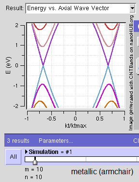
The structure of a nanotube strongly affects its electrical properties. For a given (n,m) nanotube, if n = m, the nanotube is metallic; if n − m is a multiple of 3, then the nanotube is semiconducting with a very small band gap, otherwise the nanotube is a moderate semiconductor. Thus all armchair (n = m) nanotubes are metallic, and nanotubes (6,4), (9,1), etc. are semiconducting.
Electronic devices
Nanowires can be used for transistors. Transistors are used widely as fundamental building element in today's electronic circuits. One of the key challenges of building future transistors is ensuring good gate control over the channel. Due to the high aspect ratio, if the gate dielectric is wrapped around the nanowire channel, we can get good electrostatic control of channel potential, thereby turning the transistor on and off efficiently.
Sensing using semiconductor nanowires
In an analogous way to FET devices in which the modulation of conductance (flow of electrons/holes) in the device, is controlled by electrostatic potential variation (gate-electrode) of the charge density in the conduction channel, the methodology of a Bio/Chem-FET is based on the detection of the local change in charge density, or so-called “field effect”, that characterizes the recognition event between a target molecule and the surface receptor.
This change in the surface potential influences the Chem-FET device exactly as a ‘gate’ voltage does, leading to a detectable and measurable change in the device conduction.