
Year created 1994 | ||
 | ||
Speed 655 Mbit/s (rates up to 1-3 Gbit/s possible) | ||
Low-voltage differential signaling, or LVDS, also known as TIA/EIA-644, is a technical standard that specifies electrical characteristics of a differential, serial communications protocol. LVDS operates at low power and can run at very high speeds using inexpensive twisted-pair copper cables. Since LVDS is a physical layer specification only, many data communication standards and applications use it but then add a data link layer as defined in the OSI model on top of it.
Contents
- Differential vs single ended signaling
- Applications
- Comparing serial and parallel data transmission
- LVDS transmission with 8b10b encoding
- LVDS for very high data throughput applications
- Multipoint LVDS
- SCI LVDS
- Standards
- References
LVDS was introduced in 1994, and has become popular in products such as LCD-TVs, automotive infotainment systems, industrial cameras and machine vision, notebook and tablet computers, and communications systems. The typical applications are high-speed video, graphics, video camera data transfers, and general purpose computer buses. Early on, the notebook and LCD vendors commonly used the term LVDS instead of FPD-Link when referring to their application, and the term LVDS has mistakenly become synonymous with Flat Panel Display Link in the video-display engineering vocabulary.
Differential vs. single-ended signaling
LVDS is a differential signaling system, meaning that it transmits information as the difference between the voltages on a pair of wires; the two wire voltages are compared at the receiver. In a typical implementation, the transmitter injects a constant current of 3.5 mA into the wires, with the direction of current determining the digital logic level. The current passes through a termination resistor of about 100 to 120 ohms (matched to the cable's characteristic impedance to reduce reflections) at the receiving end, and then returns in the opposite direction via the other wire. From Ohm's law, the voltage difference across the resistor is therefore about 350 mV. The receiver senses the polarity of this voltage to determine the logic level.
As long as there is tight electric- and magnetic-field coupling between the two wires, LVDS reduces the generation of electromagnetic noise. This noise reduction is due to the equal and opposite current flow in the two wires creating equal and opposite electromagnetic fields that tend to cancel each other. In addition, the tightly coupled transmission wires will reduce susceptibility to electromagnetic noise interference because the noise will equally affect each wire and appear as a common-mode noise. The LVDS receiver is unaffected by common mode noise because it senses the differential voltage, which is not affected by common mode voltage changes.
The fact that the LVDS transmitter consumes a constant current also places much less demand on the power supply decoupling and thus produces less interference in the power and ground lines of the transmitting circuit. This reduces or eliminates phenomena such as ground bounce which are typically seen in terminated single-ended transmission lines where high and low logic levels consume different currents, or in non-terminated transmission lines where a current appears abruptly during switching.
The low common-mode voltage (the average of the voltages on the two wires) of about 1.2 V allows using LVDS with a wide range of integrated circuits with power supply voltages down to 2.5 V or lower. In addition, there are variations of LVDS that use a lower common mode voltage. One example is sub-LVDS (introduced by Nokia in 2004) that uses 0.9 V typical common mode voltage. Another is Scalable Low Voltage Signaling for 400 mV (SLVS-400) specified in JEDEC JESD8-13 October 2001 where the power supply can be as low as 800 mV and common mode voltage is about 400 mV.
The low differential voltage, about 350 mV, causes LVDS to consume very little power compared to other signaling technologies. At 2.5 V supply voltage the power to drive 3.5 mA becomes 8.75 mW, compared to the 90 mW dissipated by the load resistor for an RS-422 signal.
Logic levels:
LVDS is not the only low power differential signaling system in use, others include the Fairchild Current Transfer Logic serial I/O.
Applications
LVDS became popular in the mid 1990s. Before that, computer monitor resolutions were not large enough to need such fast data rates for graphics and video. However, in 1992 Apple Computer needed a method to transfer multiple streams of digital video without overloading the existing NuBus on the backplane. Apple and National Semiconductor (NSC) created QuickRing, which was the first integrated circuit using LVDS. QuickRing was a high speed auxiliary bus for video data to bypass the NuBus in Macintosh computers. The multimedia and supercomputer applications continued to expand because both needed to move large amounts of data over links several meters long (from a disk drive to a workstation for instance).
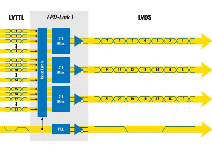
The first commercially successful application for LVDS was in notebook computers transmitting video data from graphics processing units to the flat panel displays using the Flat Panel Display Link by National Semiconductor. The first FPD-Link chipset reduced a 21-bit wide video interface plus the clock down to only 4 differential pairs (8 wires), which enabled it to easily fit through the hinge between the display and the notebook and take advantage of LVDS's low-noise characteristics and fast data rate. FPD-Link became the de facto open standard for this notebook application in the late 1990s and is still the dominant display interface today in notebook and tablet computers. This is the reason IC vendors such as Texas Instruments, Maxim, Fairchild, and Thine produce their versions of the FPD-Link chipset.
The applications for LVDS expanded to flat panel displays for consumer TVs as screen resolutions and color depths increased. To serve this application, FPD-Link chipsets continued to increase the data-rate and the number of parallel LVDS channels to meet the internal TV requirement for transferring video data from the main video processor to the display-panel's timing controller. FPD-Link (commonly called LVDS) became the de facto standard for this internal TV interconnect and remains the dominant interface for this application in 2012.
The next target application was transferring video streams through an external cable connection between a desktop computer and display, or a DVD player and a TV. NSC introduced higher performance follow-ons to FPD-Link called the LVDS Display Interface (LDI) and OpenLDI standards. These standards allow a maximum pixel clock of 112 MHz, which suffices for a display resolution of 1400 × 1050 (SXGA+) at 60 Hz refresh. A dual link can boost the maximum display resolution to 2048 × 1536 (QXGA) at 60 Hz. FPD-Link works with cable lengths up to about 5m, and LDI extends this to about 10m. However, Digital Visual Interface (DVI) using TMDS over CML signals won the standards competition and became the standard for externally connecting desktop computers to monitors, and HDMI eventually became the standard for connecting digital video sources such as DVD players to flat panel displays in consumer applications.
Another successful LVDS application is Camera Link, which is a serial communication protocol designed for computer vision applications and based on the NSC chipset called Channel Link that uses LVDS. Camera Link standardizes video interfaces for scientific and industrial products including cameras, cables, and frame grabbers. The Automated Imaging Association (AIA) maintains and administers the standard because it is the industry's global machine vision trade group.
More examples of LVDS used in computer buses are HyperTransport and FireWire, both of which trace their development back to the post-Futurebus work, which also led to SCI. In addition, LVDS is the physical layer signaling in SCSI standards (Ultra-2 SCSI and later) to allow higher data rates and longer cable lengths. Serial ATA, PCI Express, RapidIO, and SpaceWire use LVDS to allow high speed data transfer.
Intel and AMD published a press release in December 2010 stating they would no longer support the LVDS LCD-panel interface in their product lines by 2013. They are promoting Embedded DisplayPort and Internal DisplayPort as their preferred solution. However, the LVDS LCD-panel interface has proven to be the lowest cost method for moving streaming video from a video processing unit to a LCD-panel timing controller within a TV or notebook, and in February 2012 LCD TV and notebook manufacturers continue to introduce new products using the LVDS interface.
Comparing serial and parallel data transmission
LVDS works in both parallel and serial data transmission. In parallel transmissions multiple data differential pairs carry several signals at once including a clock signal to synchronize the data. In serial communications, multiple single-ended signals are serialized into a single differential pair with a data rate equal to that of all the combined single-ended channels. For example, a 7-bit wide parallel bus serialized into a single pair that will operate at 7 times the data rate of one single-ended channel. The devices for converting between serial and parallel data are the serializer and deserializer, abbreviated to SerDes when the two devices are contained in one integrated circuit.
As an example, FPD-Link actually uses LVDS in a combination of serialized and parallel communications. The original FPD-Link designed for 18-bit RGB video has 3 parallel data pairs and a clock pair, so this is a parallel communication scheme. However, each of the 3 pairs transfers 7 serialized bits during each clock cycle. So the FPD-Link parallel pairs are carrying serialized data, but use a parallel clock to recover and synchronize the data.
Serial data communications can also embed the clock within the serial data stream. This eliminates the need for a parallel clock to synchronize the data. There are multiple methods for embedding a clock into a data stream. One method is inserting 2 extra bits into the data stream as a start-bit and stop-bit to guarantee bit transitions at regular intervals to mimic a clock signal. Another method is 8b/10b encoding.
LVDS transmission with 8b/10b encoding
LVDS does not specify a bit encoding scheme because it is a physical layer standard only. LVDS accommodates any user-specified encoding scheme for sending and receiving data across an LVDS link, including 8b/10b encoded data. An 8b/10b encoding scheme embeds the clock signal information and has the added benefit of DC balance. DC balance is necessary for AC-coupled transmission paths (such as capacitive or transformer-coupled paths). There are also DC-balance encoding methods for the start bit/stop bit embedded clock, which usually include a data scrambling technique. The key point in LVDS is the physical layer signaling to transport bits across wires. It is compatible with almost all data encoding and clock embedding techniques.
LVDS for very high data-throughput applications
When a single differential pair of serial data is not fast enough there are techniques for grouping serial data channels in parallel and adding a parallel clock channel for synchronization. This is the technique used by FPD-Link. Other examples of parallel LVDS using multiple LVDS pairs and a parallel clock to synchronize are Channel Link and HyperTransport.
There is also the technique to increase the data throughput by grouping multiple LVDS-with-embedded-clock data channels together. However, this is not parallel LVDS because there is no parallel clock and each channel has its own clock information. An example of this technique is PCI Express where 2, 4, or 8 8b/10b encoded serial channels carry application data from source to destination. In this case the destination must employ a data synchronization method to align the multiple serial data channels.
Multipoint LVDS
The original LVDS standard only envisioned driving a digital signal from one transmitter to one receiver in a point-to-point topology. However, engineers using the first LVDS products soon wanted to drive multiple receivers with a single transmitter in a multipoint topology. As a result, NSC invented Bus LVDS (BLVDS) as the first variation of LVDS designed to drive multiple LVDS receivers. It uses termination resistors at each end of the differential transmission line to maintain the signal integrity. Double termination is necessary because it is possible to have one or more transmitters in the center of the bus driving signals toward receivers in both directions. The difference from standard LVDS transmitters was increasing the current output in order to drive the multiple termination resistors. In addition, the transmitters need to tolerate the possibility of other transmitters simultaneously driving the same bus.
Bus LVDS and LVDM (by TI) are de facto multipoint LVDS standards. Multipoint LVDS (MLVDS) is the TIA standard (TIA-899). The AdvancedTCA standard specified MLVDS for clock distribution across the backplane to each of the computing module boards in the system.
MLVDS has two types of receivers. Type-1 is compatible with LVDS and uses a +/− 50 mV threshold. Type-2 receivers allow Wired-Or signalling with M-LVDS devices. For M-LVDS:
SCI-LVDS
The present form of LVDS was preceded by an earlier standard initiated in Scalable Coherent Interconnect (SCI). SCI-LVDS was a subset of the SCI family of standards and specified in the IEEE 1596.3 1995 standard. The SCI committee designed LVDS for interconnecting multiprocessing systems with a high-speed and low power interface to replace positive emitter-coupled logic (PECL).
Standards
The ANSI/TIA/EIA-644-A (published in 2001) standard defines LVDS. This standard originally recommended a maximum data rate of 655 Mbit/s over twisted-pair copper wire, but data rates from 1 to 3 Gbit/s are common today on high quality transmission medium. High speed video link. Today technologies (Low Voltage Differential Signalling) for broadband digital video signal transmission in the vehicle such as LVDS used in which the signal to be transmitted for EMC reasons is coded as a differential signal. However, high-quality shielded twisted pair cables must be used together with elaborate connector systems for cabling. An alternative is the use of coaxial cables. Studies have shown that it is possible in spite of the simplified transfer medium dominate both emission and immunity in the high frequency range. Future high-speed video connections can be smaller, lighter and cheaper to realize.
Serial video transmission technologies are widely used in the automobile for linking cameras, displays and control devices. The uncompressed video data has some advantages for certain applications. Serial communication protocols now allow the transfer of data rates in the range of 3 to 4 Gbit/s and thus the control of displays with up to full HD resolution. The integration of the serializer and deserializer components in the control unit due to low demands on additional hardware and software simple and inexpensive. In contrast, require bus solutions for video transmission connection to a corresponding network controller and, if necessary resources for data compression. Since for many applications a full function network is not required throughout the video architecture and for some compounds, data compression is not feasible due to image quality loss and additional latency, bus oriented video transmission technologies are currently only partially attractive.
Figure 1. Examples of application fields of serial video transmission technologies.
Figure 1 shows an example of the video architecture of a premium-class vehicle. The serial video connections are preferably used for connecting displays that are supplied with video and MMI content of central infotainment units (head-unit and rear-Unit). Head unit and the rear unit are themselves recipients of entertainment video content (e.g. TV tuner) and assistant video data (e.g. rear view camera). Due to the high number of discrete compounds a cost and space minimization is mandatory. Show Current available technologies based on shielded differential transmission methods, both in terms of the installation space (e.g. plug size and cable cross-section) and the relatively high cost of currently widespread Star Four cable systems optimization potential. This star-quad structure - also called STQ, Shielded Twisted Quad - has established itself in spite of the slight cost disadvantage compared to the shielded twisted pair solution due to the given by the geometry significantly better RF performance in the automotive industry as a transmission medium. In recent years, the alternative of a transmission over unshielded twisted pair cables (Unshielded Twisted Pair) has been discussed often. Corresponding solutions are not sufficiently high data transfer rates available and therefore require a compression, which can be used only conditionally.