
 | ||
A symmetrical lattice is a two-port electrical wave filter in which diagonally-crossed shunt elements are present – a configuration which sets it apart from ladder networks. The component arrangement of the lattice is shown in the diagram below. The filter properties of this circuit were first developed using image impedance concepts, but later the more general techniques of network analysis were applied to it.
Contents
- Configuration
- Results from image theory
- Cascade of lattices
- The shortcomings of image theory
- Results derived by network analysis
- Conversions and equivalences
- Lattice to T see also the next section
- Unbalanced equivalents
- All pass networks
- Networks of the first and second orders
- Early history
- References
There is a duplication of components in the lattice network as the "series impedances" (instances of Za) and "shunt impedances" (instances of Zb) both occur twice, an arrangement that offers increased flexibility to the circuit designer with a variety of responses achievable. It is possible for the lattice network to have the characteristics of: a delay network, an amplitude or phase correcting network, a dispersive network or as a linear phase filter, according to the choice of components for the lattice elements.
Configuration
The basic configuration of the symmetrical lattice is shown in the left-hand diagram. A commonly used short-hand version is shown on the right, with dotted lines indicating the presence the second pair of matching impedances.
It is possible with this circuit to have the characteristic impedance specified independently of its transmission properties, a feature not available to ladder filter structures. In addition, it is possible to design the circuit to be a constant-resistance network for a range of circuit characteristics.
The lattice structure can be converted to an unbalanced form (see below), for insertion in circuits with a ground plane. Such conversions also reduce the component count and relax component tolerances.
It is possible to redraw the lattice in the Wheatstone bridge configuration (as shown in the article Zobel network). However, this is not a convenient format in which to investigate the properties of lattice filters, especially their behavior in cascade.
Results from image theory
Filter theory was initially developed from earlier studies of transmission lines. In this theory, a filter section is specified in terms of its propagation constant and image impedance (or characteristic impedance).
Specifically for the lattice, the propagation function, γ, and characteristic impedance, Z0, are defined by,
Once γ and Z0 have been chosen, solutions can be found for Za ⁄ Zb and Za × Zb from which the characteristics of Za and Zb can each be determined. (In practice, the choices for γ and Z0 are restricted to those which result in physically realisable impedances for Za and Zb). Although a filter circuit may have one or more pass-bands and possibly several stop-bands (or attenuation regions), only networks with a single pass-band are considered here.
In the pass-band of the circuit, the product Za × Zb is real (i.e. Z0 is resistive) and may be equated to R0, the terminating resistance of the filter. So
That is, the impedances behave as duals of each other within this frequency range.
In the attenuation range of the filter, the characteristic impedance of the filter is purely imaginary, and
Consequently, in order to achieve a specific characteristic, the reactances within Za and Zb are chosen so that their resonant and anti-resonant frequencies are duals of each other in the passband and match one another in the stopband. The transition region of the filter, where a change from one set of conditions to another occurs, can be made as narrow as required by increasing the complexity of Za and Zb. The phase response of the filter in the pass-band is governed by the locations (spacings) of the resonant and anti-resonant frequencies of Za and Zb.
For convenience, the normalised parameters y0 and Z0 are defined by
where normalised values za = Za ⁄ R0 and zb = Zb ⁄ R0 have been introduced. The parameter y0 is termed the index function and Z0 the characteristic impedance of the normalised network. The parameters y0 and Z0 approximate unity in the attenuation and transmission regions, respectively.
Cascade of lattices
All high-order lattice networks can be replaced by a cascade of simpler lattices, provided their characteristic impedances are all equal to that of the original and the sum of their propagation functions equals the original.
In the particular case of all-pass networks (networks which modify the phase characteristic only), any given network can always be replaced by a cascade of second-order lattices together with, possibly, one single first order lattice.
Whatever the filter requirements being considered, the reduction process results in simpler filter structures, with less stringent demands on component tolerances.
The shortcomings of image theory
The filter characteristics predicted by image theory require a correctly terminated network. As the necessary terminations are often impossible to achieve, resistors are commonly used as the terminations, resulting in a mismatched filter. Consequently, the predicted amplitude and phase responses of the circuit will no longer be as image theory predicts. In the case of a low-pass filter, for example, where the mismatch is most severe near the cut-off frequency, the transition from pass-band to stop-band is far less sharp than expected.
The figure below illustrates the problem. A lattice filter, equivalent to two sections of constant-k low-pass filter, has been derived by image methods. (The network is normalised, with L = 1 and C = 1 so R0 = √L ⁄ C = 1 and ωc = 2√L × C = 2. The left-hand figure gives the lattice circuit and the right-hand figure gives the insertion loss with the network terminated (1) resistively, and (2) in its correct characteristic impedances.
To minimise the mismatch problem, various forms of image filter end terminations were proposed by Otto Julius Zobel and others, but the inevitable compromises led to the method falling out of favour. It was replaced by the more exact methods of network analysis and network synthesis.
Results derived by network analysis
This diagram shows the general circuit for the symmetrical lattice:
Through mesh analysis or nodal analysis of the circuit, its full transfer function can be found.
The input and output impedances (Zin and Zout) of the network are given by
These equations are exact, for all realisable impedance values, unlike image theory where the propagation function only predicts performance accurately when ZS and ZL are the matching characteristic impedances of the network.
The equations can be simplified by making a number of assumptions. Firstly, networks are often sourced and terminated by resistors of the same value R0 so that ZS = ZL = R0 and the equations become
Secondly, if the impedances Za and Zb are duals of one another, so that Za × Zb = R02, then further simplification is possible:
so such networks are constant-resistance networks.
Finally, for normalised networks, with R0 = 1,
If the impedances Za and Zb (or the normalised impedances za and zb) are pure reactances, then the networks become all-pass, constant-resistance, with a flat frequency response but a variable phase response. This makes them ideal as delay networks and phase equalisers.
When resistors are present within Za and Zb then, provided the duality condition still applies, a circuit will be constant-resistance but have a variable amplitude response. One application for such circuits is as amplitude equalisers.
Conversions and equivalences
(See references)
Lattice to T (see also the next section)
This lattice-to-T conversion only gives a realisable circuit when the evaluation of Za − Zb ⁄ 2 gives positive valued components. For other situations, the bridged-T may provide a solution, as discussed in the next section.
Unbalanced equivalents
The lattice is a balanced configuration which is not suitable for some applications. In such cases it is necessary to convert the circuit to an electrically equivalent unbalanced form. This provides benefits, including reduced component count and relaxed circuit tolerances. The simple conversion procedure shown in the previous section can only be applied in a limited set of conditions – generally, some form of bridged-T circuit is necessary. Many of the conversions require the inclusion of a 1:1 ideal transformer, but there are some configurations which avoid this requirement, and one example is shown below.
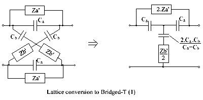
This conversion procedure starts by using the property of a lattice where a common series element in all arms can be taken outside the lattice as two series elements (as shown above). By repeatedly applying this property, components can be extracted from within the lattice structure. Finally, by means of Bartlett's bisection theorem, an unbalanced bridged-T circuit is achieved.
In the left-hand figure, the Za arm has a shunt capacitor, Ca, and the Zb arm has a series capacitor, Cb. Consequently, Za consists of Ca in parallel with Za′, and Zb consists of Cb in series with Zb′. This can be developed into the unbalanced bridged-T shown, provided Ca > Cb.
(An alternative version of this circuit has the T configuration of capacitors replaced by a Pi (or Delta) arrangement. For this T to Pi conversion, see the equations in Attenuator (electronics)).
When Cb > Ca, an alternative procedure is necessary, where common inductors are first extracted from the lattice arms. As shown, an inductor La shunts Za′ and an inductor Lb is in series with Zb′. This leads to the alternative bridged-T circuit on the right.
If La > Lb, then the negative-valued inductor can be achieved by means of mutually coupled coils. To achieve a negative mutual inductance, the two coupled inductors L1 and L2 are wound 'series-aiding'.
So finally, the bridged-T circuit takes the form
Bridged-T circuits like these may be used in delay and phase-correcting networks.
All-pass networks
(See previously quoted references to Zobel, Darlington, Bode and Guillemin. Also see Stewart and Weinberg.)
All-pass networks are an important sub-class of lattice networks. They have been used as passive lumped-element delays, as phase correctors for filter networks and in dispersive networks. They are constant-resistance networks so they can be cascaded with each other and with other circuits without introducing mismatch problems.
In the case of all-pass networks, there is no attenuation region, so the impedances Za and Zb (of the lattice) are duals of each other at all frequencies and Z0 is always resistive, equal to R0.
i.e.
For normalised networks, where R0 = 1, the transfer function T(p) can be written
and so
In practice, T(p) can be expressed as a ratio of polynomials in p, and the impedances za and zb are also ratios of polynomials in p. For the impedances to be realisable, they must satisfy Foster's reactance theorem.
Networks of the first and second orders
The two simplest all-pass networks are the first and second order lattices. These are important circuits because, as Bode pointed out, all high order all-pass lattice networks can be replaced by a cascade of second order networks with, possibly, one first order network, to give the identical response.
These two simple, normalised lattices have transfer impedances given by
These functions and the coefficients a, b and c are show in relation to components on the circuit schematics below.
The locations of the pole and zero of the first order lattice on the complex frequency plane are located at ±c on the real axis, as shown below. For the second order network, slightly more numerical manipulation is required to relate pole-zero positions to circuit values. If the poles and zeros are located at (±x ±jy) on the complex frequency plane, then the coefficients a and b can be found from
The locations of the poles and zeros on the complex frequency plane are shown below.
The unbalanced versions of these networks are found using the procedures described earlier and circuits shown below. There are two versions of the second order network: when C1 > C2 then mutually coupled coils are not required, whereas when C2 > C1 mutually coupled coils become necessary.
The circuits considered above are normalised to one ohm. To convert a circuit to have terminations of R0 ohms, multiply all L values by R0 and divide all C values by R0.
Early history
The symmetrical lattice and the ladder networks (the constant k filter and m-derived filter), were the subject of much interest in the early part of the twentieth century. At that time, the rapidly growing telephone industry had a significant influence on the development of filter theory, while seeking to increase the signal carrying capacity of telephone transmission lines. George Ashley Campbell was a key contributor to this new filter theory, as was Otto Julius Zobel. They and many colleagues worked at the laboratories of Western Electric and the American Telephone and Telegraph Co., and their work was reported in the early editions of the Bell System Technical Journal.
Campbell discussed lattice filters in his article of 1922, while other early workers with an interest in the lattice included Johnson and Bartlett. Zobel's article on filter theory and design, published at about this time, mentioned lattices only briefly, with his main emphasis on ladder networks. It was only later, when Zobel considered the simulation and equalisation of telephone transmission lines, that he gave the lattice configuration more attention. (The telephone transmission lines of the time had a balanced-pair configuration with a nominal characteristic impedance of 600 ohms, so the lattice equaliser, with its balanced structure, was particularly appropriate for use with them). Later workers, especially Hendrik Wade Bode, gave greater prominence to lattice networks in their filter designs.
In those early days, filter theory was based on image impedance concepts, or image filter theory, which was a design approach developed from the well-established studies of transmission lines. The filter was considered to be a lumped component version of a section of transmission line, and was one of many within a cascade of similar sections. As mentioned above, the weakness of the image filter approach was that the frequency response of a network was often not as predicted when the network was terminated resistively, instead of by the required image impedances. This was essentially a mismatch issue and Zobel overcame it by means of matching end sections. (see: m-derived filter, mm'-type filter, General mn-type image filter, with later work by Payne and Bode.)
Although lattice filters sometimes suffer from this same problem, a range of constant-resistance networks can avoid it altogether.
During the 1930s, as techniques in network analysis and synthesis became better developed, designing ladder filters by image methods became less popular. Even so, the concepts still found relevance in some modern designs. On the other hand, lattice networks and their circuit equivalents continue to be used in many applications.