
 | ||
Larrabee is the codename for a cancelled GPGPU chip that Intel was developing separately from its current line of integrated graphics accelerators. It is named after Larrabee State Park in Whatcom County, Washington near the town of Bellingham. The chip was to be released in 2010 as the core of a consumer 3D graphics card, but these plans were cancelled due to delays and disappointing early performance figures. The project to produce a GPU retail product directly from the Larrabee research project was terminated in May 2010. The Intel MIC multiprocessor architecture announced in 2010 inherited many design elements from the Larrabee project, but does not function as a graphics processing unit; the product is intended as a co-processor for high performance computing.
Contents
Project status
On December 4, 2009, Intel officially announced that the first-generation Larrabee would not be released as a consumer GPU product. Instead, it was to be released as a development platform for graphics and high-performance computing. The official reason for the strategic reset was attributed to delays in hardware and software development. On May 25, 2010, the Technology@Intel blog announced that Larrabee would not be released as a GPU, but instead would be released as a product for High Performance Computing competing with the Nvidia Tesla.
The project to produce a GPU retail product directly from the Larrabee research project was terminated in May 2010. The Intel MIC multiprocessor architecture announced in 2010 inherited many design elements from the Larrabee project, but does not function as a graphics processing unit; the product is intended as a co-processor for high performance computing. The prototype card was named Knights Ferry, a production card built at a 22 nm process named Knights Corner was planned for production in 2012 or later.
Comparison with competing products
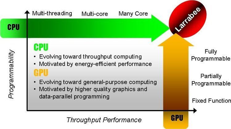
Larrabee can be considered a hybrid between a multi-core CPU and a GPU, and has similarities to both. Its coherent cache hierarchy and x86 architecture compatibility are CPU-like, while its wide SIMD vector units and texture sampling hardware are GPU-like.
As a GPU, Larrabee would have supported traditional rasterized 3D graphics (Direct3D & OpenGL) for games. However, Larrabee's hybrid of CPU and GPU features should also have been suitable for general purpose GPU (GPGPU) or stream processing tasks. For example, Larrabee might have performed ray tracing or physics processing, in real time for games or offline for scientific research as a component of a supercomputer.
Larrabee's early presentation drew some criticism from GPU competitors. At NVISION 08, an Nvidia employee called Intel's SIGGRAPH paper about Larrabee "marketing puff" and quoted an industry analyst (Peter Glaskowsky) who speculated that the Larrabee architecture was "like a GPU from 2006". As of June 2009, prototypes of Larrabee have been claimed to be on par with the Nvidia GeForce GTX 285. Justin Rattner, Intel CTO, delivered a keynote at the Supercomputing 2009 conference on November 17, 2009. During his talk he demonstrated an overclocked Larrabee processor topping one teraFLOPS in performance. He claimed this was the first public demonstration of a single chip system exceeding one teraFLOPS. He pointed out this was early silicon thereby leaving open the question on eventual performance for Larrabee. Because this was only one fifth that of available competing graphics boards, Larrabee was cancelled "as a standalone discrete graphics product" on December 4, 2009.
Differences with current GPUs
Larrabee was intended to differ from older discrete GPUs such as the GeForce 200 Series and the Radeon 4000 series in three major ways:
This had been expected to make Larrabee more flexible than current GPUs, allowing more differentiation in appearance between games or other 3D applications. Intel's SIGGRAPH 2008 paper mentioned several rendering features that were difficult to achieve on current GPUs: render target read, order-independent transparency, irregular shadow mapping, and real-time raytracing.
More recent GPUs such as ATI's Radeon HD 5xxx and Nvidia's GeForce 400 Series feature increasingly broad general-purpose computing capabilities via DirectX11 DirectCompute and OpenCL, as well as Nvidia's proprietary CUDA technology, giving them many of the capabilities of the Larrabee.
Differences with CPUs
The x86 processor cores in Larrabee differed in several ways from the cores in current Intel CPUs such as the Core 2 Duo or Core i7:
Theoretically Larrabee's x86 processor cores were able to run existing PC software, or even operating systems. A different version of Larrabee might sit in motherboard CPU sockets using QuickPath, but Intel never announced any plans for this. Though Larrabee Native's C/C++ compiler included auto-vectorization and many applications were able to execute correctly after having been recompiled, maximum efficiency was expected to have required code optimization using C++ vector intrinsics or inline Larrabee assembly code. However, as in all GPGPU, not all software would have benefited from utilization of a vector processing unit. One tech journalism site claims that Larrabee graphics capabilities were planned to be integrated in CPUs based on the Haswell microarchitecture.
Comparison with the Cell Broadband Engine
Larrabee's philosophy of using many small, simple cores was similar to the ideas behind the Cell processor. There are some further commonalities, such as the use of a high-bandwidth ring bus to communicate between cores. However, there were many significant differences in implementation which were expected to make programming Larrabee simpler.
Comparison with Intel GMA
Intel began integrating a line of GPUs onto motherboards under the Intel GMA brand in 2004. Being integrated onto motherboards (newer versions, such as those released with Sandy Bridge, are incorporated onto the same die as the CPU) these chips were not sold separately. Though the low cost and power consumption of Intel GMA chips made them suitable for small laptops and less demanding tasks, they lack the 3D graphics processing power to compete with contemporary Nvidia and AMD/ATI GPUs for a share of the high-end gaming computer market, the HPC market, or a place in popular video game consoles. In contrast, Larrabee was to be sold as a discrete GPU, separate from motherboards, and was expected to perform well enough for consideration in the next generation of video game consoles.
The team working on Larrabee was separate from the Intel GMA team. The hardware was designed by a newly formed team at Intel's Hillsboro, Oregon site, separate from those that designed the Nehalem. The software and drivers were written by a newly formed team. The 3D stack specifically was written by developers at RAD Game Tools (including Michael Abrash).
The Intel Visual Computing Institute will research basic and applied technologies that could be applied to Larrabee-based products.
Preliminary performance data
Intel's SIGGRAPH 2008 paper describes cycle-accurate simulations (limitations of memory, caches and texture units was included) of Larrabee's projected performance. Graphs show how many 1 GHz Larrabee cores are required to maintain 60 frame/s at 1600x1200 resolution in several popular games. Roughly 25 cores are required for Gears of War with no antialiasing, 25 cores for F.E.A.R with 4x antialiasing, and 10 cores for Half-Life 2: Episode 2 with 4x antialiasing. It is likely that Larrabee will run faster than 1 GHz, so these numbers do not represent actual Larrabee cores, rather virtual timeslices of such. Another graph shows that performance on these games scales nearly linearly with the number of cores up to 32 cores. At 48 cores the performance drops to 90% of what would be expected if the linear relationship continued.
A June 2007 PC Watch article suggested that the first Larrabee chips would feature 32 x86 processor cores and come out in late 2009, fabricated on a 45 nanometer process. Chips with a few defective cores due to yield issues would be sold as a 24-core version. Later in 2010, Larrabee would be shrunk for a 32 nanometer fabrication process to enable a 48 core version.
The last statement of performance can be calculated (theoretically this is maximum possible performance) as follows: 32 cores × 16 single-precision float SIMD/core × 2 FLOP (fused multiply-add) × 2 GHz = 2 TFLOPS
Public demonstrations
The first public demonstration of the Larrabee architecture took place at the Intel Developer Forum in San Francisco on September 22, 2009. An early Larrabee port of the former CPU-based research project Quake Wars: Ray Traced has been shown in real-time. The scene contained a ray traced water surface that reflected the surrounding objects like a ship and several flying vehicles accurately.
The second demo was given at the SC09 conference in Portland at November 17, 2009 during a keynote by Intel CTO Justin Rattner. A Larrabee card was able to achieve 1006 GFLops in the SGEMM 4Kx4K calculation.