
 | ||
Jacobs institute for design innovation ribbon cutting w oski
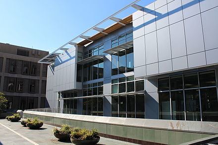
The Jacobs Institute for Design Innovation is a building on the UC Berkeley campus, part of the UC Berkeley College of Engineering. Construction began in August 2014 with a $20 million gift from the Paul and Stacy Jacobs Foundation. The ribbon-cutting ceremony took place on August 20, 2015, with speeches by speeches by various UC Berkeley administrators, Ellen Lupton, Paul E. Jacobs, executive chairman of Qualcomm, and the building opened for instruction on September 16. The 24,000-square-foot building was constructed at a cost of $25 million, funded by philanthropy.
Contents
- Jacobs institute for design innovation ribbon cutting w oski
- Clip elizabeth gerber jacobs institute for design innovation
- References
The building includes open student studio space on the first floor, two classrooms on the second floor, and a large conference room on the third floor. It has design studios with shop tools and rapid prototyping equipment.