
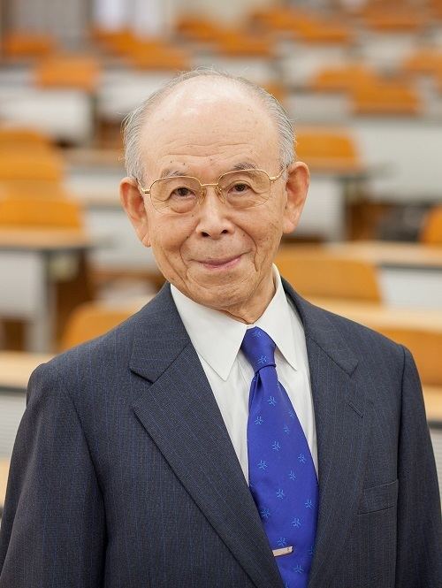
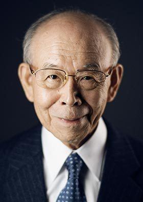
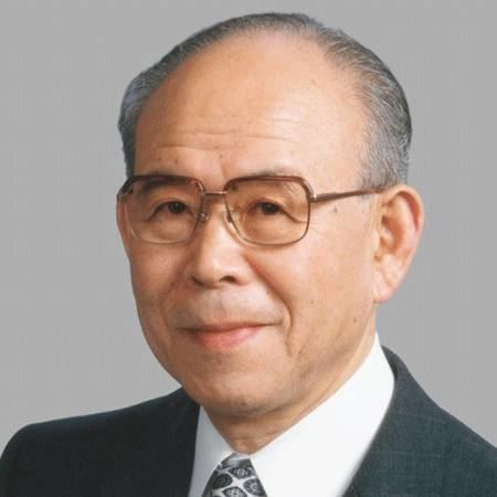
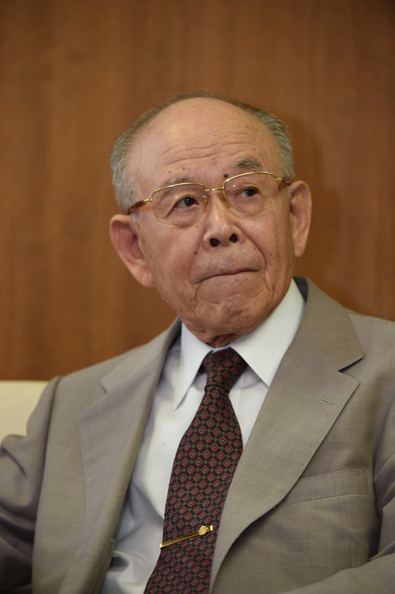
Name Isamu Akasaki Role Scientist | Spouse Ryoko Akasaki | |
 | ||
Institutions Meijo UniversityNagoya University Alma mater Kyoto UniversityNagoya University Notable awards Asahi Prize (2001)Takeda Award (2002)IEEE Edison Medal (2011)Nobel Prize in Physics (2014)Charles Stark Draper Prize (2015) Similar People Hiroshi Amano, Shuji Nakamura, William E Moerner, Eric Betzig, John O'Keefe | ||
i was overwhelmed so many congratulations isamu akasaki on being awarded the nobel prize
Isamu Akasaki (赤崎 勇, Akasaki Isamu, born January 30, 1929) is a Japanese physicist, specializing in the field of semiconductor technology and Nobel Prize laureate, best known for inventing the bright gallium nitride (GaN) p-n junction blue LED in 1989 and subsequently the high-brightness GaN blue LED as well.
Contents
- i was overwhelmed so many congratulations isamu akasaki on being awarded the nobel prize
- Message from isamu akasaki the 2009 kyoto prize
- Career
- Nagoya University Akasaki Institute
- Professional record
- National
- References
For this and other achievements Isamu Akasaki was awarded the Kyoto Prize in Advanced Technology in 2009 and the IEEE Edison Medal in 2011. He was also awarded the 2014 Nobel prize in Physics, together with Hiroshi Amano and Shuji Nakamura, "for the invention of efficient blue light-emitting diodes, which has enabled bright and energy-saving white light sources".
Message from isamu akasaki the 2009 kyoto prize
Career
Born in Kagoshima Prefecture, Akasaki graduated from Kyoto University in 1952, and obtained a Dr.Eng. degree in Electronics from Nagoya University in 1964. He started working on GaN-based blue LEDs in the late 1960s. Step by step, he improved the quality of GaN crystals and device structures at Matsushita Research Institute Tokyo, Inc.(MRIT), where he decided to adopt metalorganic vapor phase epitaxy (MOVPE) as the preferred growth method for GaN.
In 1981 he started afresh the growth of GaN by MOVPE at Nagoya University, and in 1985 he and his group succeeded in growing high-quality GaN on sapphire substrate by pioneering the low-temperature (LT) buffer layer technology.
This high-quality GaN enabled them to discover p-type GaN by doping with magnesium (Mg) and subsequent activation by electron irradiation (1989), to produce the first GaN p-n junction blue/UV LED (1989), and to achieve conductivity control of n-type GaN (1990) and related alloys (1991) by doping with silicon (Si), enabling the use of hetero structures and multiple quantum wells in the design and structure of more efficient p-n junction light emitting structures.
They achieved stimulated emission from the GaN firstly at room temperature in 1990, and developed in 1995 the stimulated emission at 388 nm with pulsed current injection from high-quality AlGaN/GaN/GaInN quantum well device. They verified quantum size effect (1991) and quantum confined Stark effect (1997) in nitride system, and in 2000 showed theoretically the orientation dependence of piezoelectric field and the existence of non-/semi-polar GaN crystals, which have triggered today’s worldwide efforts to grow those crystals for application to more efficient light emitters.
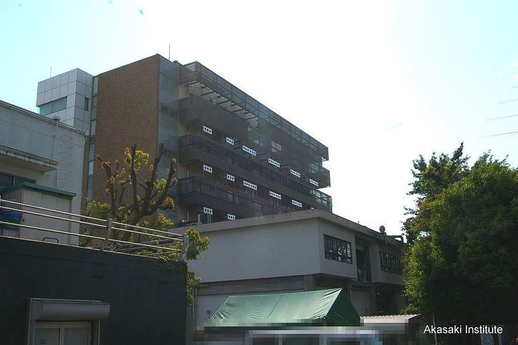
Nagoya University Akasaki Institute
Professor Akasaki’s patents were produced from these inventions, and the patents have been rewarded as royalties. Nagoya University Akasaki Institute opened on October 20, 2006. The cost of construction of the institute was covered with the patent royalty income to the university, which was also used for a wide range of activities in Nagoya University. The institute consists of an LED gallery to display the history of blue LED research/developments and applications, an office for research collaboration, laboratories for innovative research, and Professor Akasaki's office on the top sixth floor. The institute is situated in the center of the collaboration research zone in Nagoya University Higashiyama campus.