Kalpana Kalpana (Editor)

Intel 4040

Updated on
Edit
Like
Comment
Share on FacebookTweet on TwitterShare on LinkedInShare on Reddit
Produced
  
From 1974 to 1981

Max. CPU clock rate
  
500 kHz to 740 kHz

Instruction set
  
4-bit BCD oriented

Common manufacturer(s)
  
Intel

Min. feature size
  
10μm

Predecessor
  
Intel 4004 Intel 8008

Intel 4040

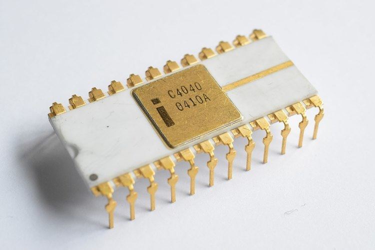
The Intel 4040 microprocessor was the successor to the Intel 4004. It was introduced in 1974. The 4040 employed a 10 μm silicon gate enhancement load PMOS technology, was made up of 3,000 transistors and could execute approximately 60,000 instructions per second.

Contents

New features

  • Interrupt
  • Single Step
  • Extensions

  • Instruction Set expanded to 60 instructions
  • Program memory expanded to 8 KB (13-bit address space)
  • Registers expanded to 24
  • Subroutine stack expanded to 7 levels deep
  • Data Bus: 4-bit
    Address Bus: 12-bit
    Voltage: +15V

    Designers

    Federico Faggin proposed the project, formulated the architecture and led the design. The detailed design was done by Tom Innes (Tinnes of Bristol).

    New support chips

  • 4201 – Clock Generator 500 to 740 kHz using 4 to 5.185 MHz crystals
  • 4308 – 1 KB ROM
  • 4207 – General Purpose byte Output port
  • 4209 – General Purpose byte Input port
  • 4211 – General Purpose byte I/O port
  • 4289 – Standard Memory Interface (replaces 4008/4009)
  • 4702 – 256 byte UVEPROM
  • 4316 – 2 KB ROM
  • 4101 – 256 4-bit word RAM
  • Production

    Philippines

    References

    Intel 4040 Wikipedia


    Similar Topics