
 | ||
Indium gallium nitride (InGaN, InxGa1−xN) is a semiconductor material made of a mix of gallium nitride (GaN) and indium nitride (InN). It is a ternary group III/group V direct bandgap semiconductor. Its bandgap can be tuned by varying the amount of indium in the alloy. InxGa1−xN has a direct bandgap span from the infrared (0.69 eV) for InN to the ultraviolet (3.4 eV) of GaN. The ratio of In/Ga is usually between 0.02/0.98 and 0.3/0.7.
Contents
LEDs

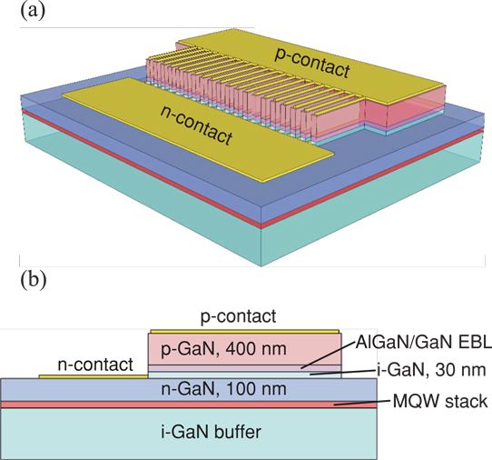
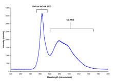
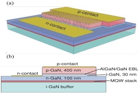
Indium gallium nitride is the light-emitting layer in modern blue and green LEDs and often grown on a GaN buffer on a transparent substrate as, e.g. sapphire or silicon carbide. It has a high heat capacity and its sensitivity to ionizing radiation is low (like other group III nitrides), making it also a potentially suitable material for solar photovoltaic devices, specifically for arrays for satellites.
It is theoretically predicted that spinodal decomposition of indium nitride should occur for compositions between 15% and 85%, leading to In-rich and Ga-rich InGaN regions or clusters. However, only a weak phase segregation has been observed in experimental local structure studies. Other experimental results using cathodoluminescence and photoluminescence excitation on low In-content InGaN multi-quantum wells have demonstrated that providing correct material parameters of the InGaN/GaN alloys, theoretical approaches for AlGaN/GaN systems also applies to InGaN nanostructures.
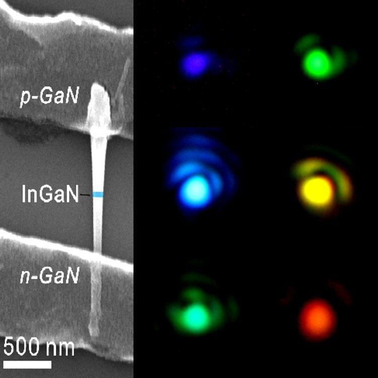
GaN is a defect-rich material with typical dislocation densities exceeding 108 cm−2. Light emission from InGaN layers grown on such GaN buffers used in blue and green LEDs is expected to be attenuated because of non-radiative recombination at such defects. Nevertheless, InGaN quantum wells, are efficient light emitters in green, blue, white and ultraviolet light-emitting diodes and diode lasers. The indium-rich regions have a lower bandgap than the surrounding material and create regions of reduced potential energy for charge carriers. Electron-hole pairs are trapped there and recombine with emission of light, instead of diffusing to crystal defects where the recombination is non-radiative. Also, self-consistent computer simulations have shown that radiative recombination is focused where regions are rich of indium.
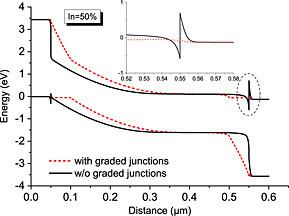
The emitted wavelength, dependent on the material's band gap, can be controlled by the GaN/InN ratio, from near ultraviolet for 0.02In/0.98Ga through 390 nm for 0.1In/0.9Ga, violet-blue 420 nm for 0.2In/0.8Ga, to blue 440 nm for 0.3In/0.7Ga, to red for higher ratios and also by the thickness of the InGaN layers which are typically in the range of 2–3 nm. However, atomistic simulations results have shown that emission energies have a minor dependence on small variations of device dimensions. Studies based on device simulation have shown that it could be possible to increase InGaN/GaN LED efficiency using band gap engineering, especially for green LEDs.
Photovoltaics
The ability to perform bandgap engineering with InGaN over a range that provides a good spectral match to sunlight, makes InGaN suitable for solar photovoltaic cells. It is possible to grow multiple layers with different bandgaps, as the material is relatively insensitive to defects introduced by a lattice mismatch between the layers. A two-layer multijunction cell with bandgaps of 1.1 eV and 1.7 eV can attain a theoretical 50% maximum efficiency, and by depositing multiple layers tuned to a wide range of bandgaps an efficiency up to 70% is theoretically expected.
Significant photoresponse was obtained from experimental InGaN single-junction devices. In addition to controlling the optical properties, which results in band gap engineering, photovoltaic device performance can be improved by engineering the microstructure of the material to increase the optical path length and provide light trapping. Growing nanocolumns on the device can further result in resonant interaction with light, and InGaN nanocolumns have been successfully deposited on SiO
2 using plasma enhanced evaporation.
Metal-modulated epitaxy allows controlled atomic layer-by-layer growth of thin films with almost ideal characteristics enabled by strain relaxation at the first atomic layer. The crystal's lattice structures match up, resembling a perfect crystal, with corresponding luminosity. The crystal had indium content ranging from x ∼ 0.22 to 0.67. Significant improvement in the crystalline quality and optical properties began at x ∼ 0.6. Films were grown at ∼400 °C to facilitate indium incorporation and with precursor modulation to enhance surface morphology and metal adlayer diffusion. These findings should contribute to the development of growth techniques for nitride semiconductors under high lattice misfit conditions.
Quantum heterostructures
Quantum heterostructures are often built from GaN with InGaN active layers. InGaN can be combined with other materials, e.g. GaN, AlGaN, on SiC, sapphire and even silicon.
Safety and toxicity
The toxicology of InGaN has not been fully investigated. The dust is an irritant to skin, eyes and lungs. The environment, health and safety aspects of indium gallium nitride sources (such as trimethylindium, trimethylgallium and ammonia) and industrial hygiene monitoring studies of standard MOVPE sources have been reported recently in a review.