
 | ||
A heterojunction is the interface that occurs between two layers or regions of dissimilar crystalline semiconductors. These semiconducting materials have unequal band gaps as opposed to a homojunction. It is often advantageous to engineer the electronic energy bands in many solid-state device applications, including semiconductor lasers, solar cells and transistors ("heterotransistors") to name a few. The combination of multiple heterojunctions together in a device is called a heterostructure, although the two terms are commonly used interchangeably. The requirement that each material be a semiconductor with unequal band gaps is somewhat loose, especially on small length scales, where electronic properties depend on spatial properties. A more modern definition of heterojunction is the interface between any two solid-state materials, including crystalline and amorphous structures of metallic, insulating, fast ion conductor and semiconducting materials.
Contents
- Manufacture and applications
- Energy band alignment
- Effective mass mismatch at heterojunctions
- Nanoscale heterojunctions
- References
In 2000, the Nobel Prize in physics was awarded jointly to Herbert Kroemer (University of California, Santa Barbara, California, USA) and Zhores I. Alferov (Ioffe Institute, Saint Petersburg, Russia) for "developing semiconductor heterostructures used in high-speed- and opto-electronics".
Manufacture and applications
Heterojunction manufacturing generally requires the use of molecular beam epitaxy (MBE) or chemical vapor deposition (CVD) technologies in order to precisely control the deposition thickness and create a cleanly lattice-matched abrupt interface.
Despite their expense, heterojunctions have found use in a variety of specialized applications where their unique characteristics are critical:
Energy band alignment
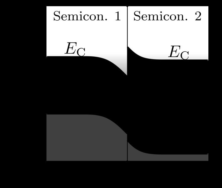
The behaviour of a semiconductor junction depends crucially on the alignment of the energy bands at the interface. Semiconductor interfaces can be organized into three types of heterojunctions: straddling gap (type I), staggered gap (type II) or broken gap (type III) as seen in the figure. Away from the junction, the band bending can be computed based on the usual procedure of solving Poisson's equation.
Various models exist to predict the band alignment.
The typical method for measuring band offsets is by calculating them from measuring exciton energies in the luminescence spectra.
Effective mass mismatch at heterojunctions
When a heterojunction is formed by two different semiconductors, a quantum well can be fabricated due to difference in band structure. In order to calculate the static energy levels within the achieved quantum well, understanding variation or mismatch of the effective mass across the heterojunction becomes substantial. The quantum well defined in the heterojunction can be treated as a finite well potential with width of
Nanoscale heterojunctions
In quantum dots the band energies are dependent on crystal size due to the quantum size effects. This enables band offset engineering in nanoscale heterostructures. It is possible to use the same materials but change the type of junction, say from straddling (type I) to staggered (type II), by changing the size or thickness of the crystals involved. The most common nanoscale heterostructure system is ZnS on CdSe (CdSe@ZnS) which has a straddling gap (type I) offset. In this system the much larger band gap ZnS passivates the surface of the fluorescent CdSe core thereby increasing the quantum efficiency of the luminescence. There is an added bonus of increased thermal stability due to the stronger bonds in the ZnS shell as suggested by its larger band gap. Since CdSe and ZnS both grow in the zincblende crystal phase and are closely lattice matched, core shell growth is preferred. In other systems or under different growth conditions it may be possible to grow anisotropic structures such as the one seen in the image on the right.
It has been shown that the driving force for charge transfer between conduction bands in these structures is the conduction band offset. By decreasing the size of CdSe nanocrystals grown on TiO2, Robel et al. found that electrons transferred faster from the higher CdSe conduction band into TiO2. In CdSe the quantum size effect is much more pronounced in the conduction band due to the smaller effective mass than in the valence band, and this is the case with most semiconductors. Consequently, engineering the conduction band offset is typically much easier with nanoscale heterojunctions. For staggered (type II) offset nanoscale heterojunctions, photoinduced charge separation can occur since there the lowest energy state for holes may be on one side of the junction whereas the lowest energy for electrons is on the opposite side. It has been suggested that anisotropic staggered gap (type II) nanoscale heterojunctions may be used for photocatalysis, specifically for water splitting with solar energy.